Engineering and Technology
Wearable perovskite solar cells by aligned liquid crystal elastomers
Z. Huang, L. Li, et al.
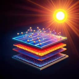
This groundbreaking research by Zengqi Huang and colleagues introduces a liquid crystal elastomer interlayer to enhance the efficiency and durability of flexible perovskite solar cells. Achieving efficiencies of 23.26% in rigid and 22.10% in flexible forms, these cells not only exhibit impressive performance but also integrate seamlessly into wearable devices for virtual reality applications.
~3 min • Beginner • English
Introduction
Perovskite solar cells (PSCs) are promising for next-generation photovoltaics due to high efficiencies (>25%), low weight, flexibility, and low-temperature processing. However, commercialization is hindered by limited operational stability and mechanical endurance, largely stemming from interfacial defects, especially at the bottom electron transport layer (ETL)/perovskite interface where deep-level defects cause hysteresis and irreversible degradation. In planar architectures with large interfacial areas, efficient charge extraction with minimal interfacial recombination is critical. Existing approaches such as interfacial layers, interpenetrating interfaces, scaffolds, and additives can mitigate defects, and self-assembled monolayers (SAMs) are a simple effective approach to reduce transport losses and recombination. Yet SAMs on flexible substrates suffer from defects due to substrate roughness and deposition, undermining performance and stability. Cross-linked SAMs via silanization improve hysteresis and stability while maintaining mechanical tolerance, but introduce a trade-off between passivation quality (VOC) and series resistance (FF) due to heterogeneous contact of silanes. Therefore, an interfacial strategy that simultaneously provides strong passivation and good carrier conductivity without trade-offs is urgently needed. Liquid crystalline elastomers (LCEs), with anisotropic mesogenic order and elastic polymer networks, offer tunable alignment and have improved electrical and mechanical properties in composites, suggesting potential to form ordered, tough charge-transfer channels in flexible PSCs. This work introduces an aligned LCE interlayer at the SnO2/perovskite bottom interface to enhance charge extraction, reduce recombination, and improve reliability and mechanical robustness of rigid and flexible PSCs.
Literature Review
Multiple interfacial engineering strategies have been explored to reduce defects and recombination at the ETL/perovskite interface: introducing interfacial layers; creating interpenetrating interfaces; employing scaffolding; and using additives. Self-assembled monolayers (SAMs) can effectively minimize charge-transport losses and suppress recombination, but on flexible substrates SAMs suffer from defects arising from substrate roughness and deposition processes. Cross-linked SAMs formed via silanization reduce hysteresis and improve operational stability while preserving mechanical tolerance, yet they often introduce a trade-off between passivation (improving VOC) and increased series resistance (degrading FF) due to heterogeneous contact. LCEs, lightly cross-linked networks with self-assembled mesogens, have demonstrated anisotropic electrical properties and mechanical elasticity in composites (e.g., with carbon nanotubes), indicating their potential to provide ordered, conductive, and mechanically tough interfacial layers in flexible optoelectronic devices, motivating their application here as an aligned interlayer to toughen the ETL/perovskite interface.
Methodology
An aligned liquid crystal elastomer (LCE) interlayer was synthesized and integrated at the SnO2/perovskite (bottom) interface of planar n–i–p PSCs. LC oligomer synthesis: liquid crystal diacrylate (RM257) and 1,3-pentanedithiol were reacted (1:2 molar ratio) in CH2Cl2 with DBU catalyst at room temperature overnight, followed by acid washing, drying, filtration, and solvent removal to obtain dithiol-terminated LC oligomers. LCE formation: RM257 and LC oligomers were mixed at 1:1 molar ratio in toluene with 2 wt% DMPA (photoinitiator) and 0.2 wt% BHT (inhibitor). Solutions (0.05–0.5 mg mL−1) were spin-coated on SnO2-coated substrates (6000 rpm, 30 s), annealed at 150 °C for 30 min to form uniform LC texture, and UV-exposed (10 min) to induce oxygen-mediated thiol–acrylate click photopolymerization, instant-locking mesogenic alignment into a thin (~9.6 nm) LCE film. Device fabrication: Rigid devices on ITO/glass used spin-coated SnO2 (2.67%, 5000 rpm, 30 s; 150 °C, 30 min). Flexible devices used PEN/ITO supported on PDMS; SnO2 was annealed at 120 °C for 30 min. The LCE interlayer was deposited as above. The perovskite precursor (CsFAMA: 1.25 M PbI2, 0.87 M FAI, 0.25 M MAI, 0.13 M CsI in DMF/DMSO 4:1; 0.02 wt% PU for flexible substrates) was spin-coated (1000 rpm 10 s, then 5000 rpm 30 s; chlorobenzene antisolvent drip at 32 s), then annealed (100 °C 1 min; 120 °C 30 min). HTL Spiro-OMeTAD (with Li-TFSI and tBP dopants) was spin-coated (3000 rpm, 30 s). Ag (90 nm) was thermally evaporated as the top electrode. Characterization: LCE formation and alignment were verified by FTIR (acrylate conversion), POM (birefringence), AFM (periodic morphology), and GIWAXS (molecular stacking). Perovskite crystallinity and orientation were assessed by XRD and GIWAXS. Surface wettability/contact angle measured on SnO2 vs SnO2/LCE. Optical/electronic properties were evaluated by steady-state PL and time-resolved PL (bi-exponential fits to extract τ1 and τ2). Energy levels were probed by UPS to determine CBM/VBM. AFM/KPFM mapped surface potentials and uniformity. Conductivity and uniformity of ETL/interlayers were tested via I–V on ITO/ETL/Ag structures across multiple regions and compared with APTES and LC oligomer controls. Electron-only devices were used for SCLC analysis to extract trap-filling limit voltage (VTFL) and trap density; thermal admittance spectroscopy provided trap density of states (tDOS). XPS on ion-milled bottom perovskite surfaces examined chemical states (Pb 4f). Device performance: J–V (forward/reverse scans), EQE, hysteresis index, intensity-dependent J–V (recombination analysis), transient photovoltage (TPV). Operational stability: unencapsulated MPP tracking under AM 1.5 G in ambient and under flowing N2 (T80), ISOS protocol continuous MPP tracking; time-evolution GIWAXS/XRD under illumination; FIB-SEM and top-view SEM to assess interfacial degradation/voids. Flexible device mechanical tests: J–V at various bending angles/radii, cycling durability (up to 5000 bends), residual stress calculation (function fitting per Supplementary Note), and morphology evolution during bending. System integration: LCE-based flexible PSCs powered a wearable haptic device with microneedle sensor arrays; continuous photovoltage tracking under ambient light; temperature modulation tests (20–35 °C); mechanical bending under illumination to assess voltage variation and recovery.
Key Findings
- Introducing an aligned LCE interlayer at the SnO2/perovskite interface enhances charge extraction and suppresses interfacial recombination, yielding high efficiencies: rigid PSC PCE up to 23.26% (VOC 1.17 V, JSC 24.79 mA cm−2, FF 0.80) with low hysteresis index (0.030); flexible PSC PCE up to 22.10% (VOC 1.15 V, JSC 24.69 mA cm−2, FF 0.780), with only ~5% efficiency loss from rigid to flexible substrates.
- Perovskite crystallinity and orientation improved: XRD FWHM of (001) reduced from 0.167 (SnO2) to 0.148 (SnO2/LCE); PbI2 peak at 12.6° diminished; (001)/(012) intensity ratio increased; GIWAXS showed stronger out-of-plane (001) orientation.
- Surface energetics favored nucleation: contact angle decreased from 19.6° (SnO2) to 13.4° (SnO2/LCE), reducing heterogeneous nucleation barrier and promoting dense films.
- Charge transfer and energy alignment: PL/TRPL indicated most efficient charge extraction on SnO2/LCE; UPS showed CBM/VBM at −4.43 eV/−8.04 eV for SnO2/LCE, with CBM downshift facilitating electron injection versus pristine SnO2 (CBM −4.01 eV).
- Uniform charge transport channel: KPFM revealed negligible surface potential variation on SnO2/LCE versus −17 mV on SnO2; ITO/ETL/Ag I–V curves were spatially consistent only with LCE.
- Defect suppression: Electron-only SCLC VTFL reduced from 0.41 V (SnO2) to 0.17 V (SnO2/LCE), decreasing trap density from 1.61 × 10^6 cm−3 to 6.68 × 10^5 cm−3; tDOS reduced across defect energies; XPS indicated 0.2 eV lower Pb 4f binding energy consistent with sulfur coordination/passivation of undercoordinated Pb2+.
- Recombination analysis: Intensity-dependent J–V gave smaller slope at VOC (1.50 kT/q vs 1.92 kT/q) and higher α near JSC (0.994) for LCE devices, indicating suppressed trap-assisted and bimolecular recombination; TPV decay time increased (0.17 ms vs 0.05 ms), indicating slower recombination.
- Operational stability: Under AM 1.5 G MPP tracking (ambient), reference lost 80% PCE in 19 h; LCE devices retained 92% after 100 h. Under flowing N2, unencapsulated LCE devices showed T80 > 1570 h (vs 510 h reference). ISOS MPP tracking retained 85% after 1443 h with T80 > 500 h. Time-evolution GIWAXS/XRD showed LCE suppresses lattice shrinkage and phase segregation at (012) during operation.
- Mechanical robustness: Flexible LCE devices retained 86% of initial efficiency after 5000 bending cycles; reduced residual tensile stress in perovskite with LCE (12.01 MPa) vs reference (25.52 MPa); SEM/FIB-SEM showed fewer voids/delamination and better structural integrity at the SnO2/perovskite interface with LCE.
- System demonstration: LCE-based flexible PSCs powered a wearable haptic device with microneedle sensor arrays; stable photovoltage under ambient light (~−1.03 V); reliable operation under bending with reversible photovoltage changes due to illumination area variations.
Discussion
The aligned LCE interlayer forms a robust, uniform, and conductive charge-transfer channel at the SnO2/perovskite bottom interface. Its mesogenic order, locked by photopolymerization, improves wetting and nucleation, yielding denser, preferentially oriented perovskite grains with fewer pinholes and reduced PbI2 residue. Energy level alignment (CBM downshift) and uniform surface potential facilitate efficient electron extraction, while chemical interaction (thiol-derived sulfur coordination) passivates undercoordinated Pb2+ sites, lowering trap densities. Consequently, both trap-assisted and bimolecular recombination are suppressed, as evidenced by PL/TRPL, intensity-dependent J–V, and TPV analyses. The LCE interlayer also mechanically toughens the interface, reducing residual stress and preventing light-induced interfacial delamination and phase segregation, leading to markedly improved operational stability (T80 > 1570 h under N2) and bending durability (86% PCE retention after 5000 cycles). These interfacial and mechanical advantages translate into state-of-the-art efficiencies for both rigid and flexible PSCs and enable reliable integration into wearable electronic systems.
Conclusion
This work introduces an aligned liquid crystal elastomer interlayer at the SnO2/perovskite interface to simultaneously enhance electronic contact, suppress defects and recombination, and toughen interfacial mechanics. The approach yields high-efficiency PSCs (23.26% rigid; 22.10% flexible), greatly improves operational stability (unencapsulated T80 > 1570 h under N2), and provides excellent mechanical endurance (86% PCE retention after 5000 bending cycles). The interlayer also enables stable operation in a wearable haptic device demonstration, highlighting its potential for practical flexible electronics. The findings offer an effective strategy for designing reliable interfaces in perovskite photovoltaics and flexible devices.
Limitations
Related Publications
Explore these studies to deepen your understanding of the subject.

