
Engineering and TechnologyNature Communications
An inorganic-blended p-type semiconductor with robust electrical and mechanical properties
Y. Meng, W. Wang, et al.
Discover the groundbreaking research by You Meng and colleagues on the innovative tellurium-selenium-oxygen (TeSeO) blending strategy, which activates hole transport in inorganic semiconductors. With tunable bandgaps and remarkable hole mobility, TeSeO films pave the way for high-performance photodetectors that exhibit flexibility, ultrafast responses, and exceptional responsivity.
Related Publications
Explore these studies to deepen your understanding
Adjacent work that informs or extends this paper's methodology and findings.

Engineering and Technology
Hollow silica reinforced magnesium nanocomposites with enhanced mechanical and biological properties with computational modeling analysis for mandibular reconstruction
S. Prasadh, V. Manakari, et al.
Medicine and Health
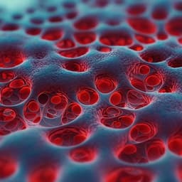
Superporous sponge prepared by secondary network compaction with enhanced permeability and mechanical properties for non-compressible hemostasis in pigs
T. Jiang, S. Chen, et al.

Engineering and Technology
Self-growing photonic composites with programmable colors and mechanical properties
J. Xue, X. Yin, et al.

Medicine and Health
An injectable photopolymerized hydrogel with antimicrobial and biocompatible properties for infected skin regeneration
A. Sun, X. He, et al.


