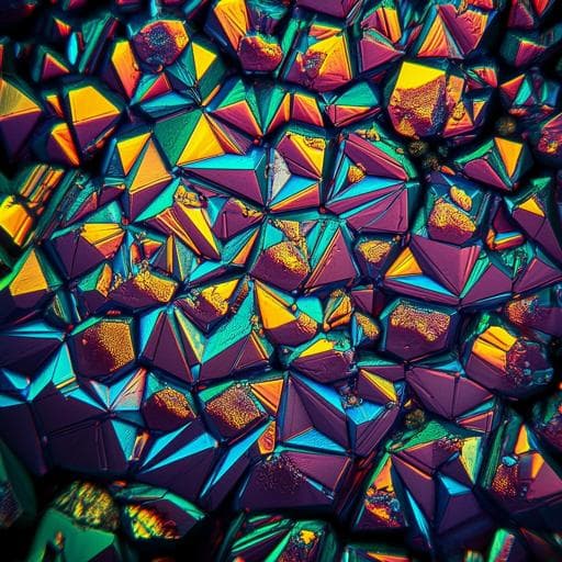
Controlled on-chip fabrication of large-scale perovskite single crystal arrays for high-performance laser and photodetector integration
Z. Xu, X. Han, et al.
Explore these studies to deepen your understanding
Adjacent work that informs or extends this paper's methodology and findings.
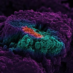
Bottom-up construction of low-dimensional perovskite thick films for high-performance X-ray detection and imaging
S. Dong, Z. Fan, et al.
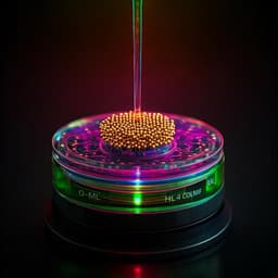
Monolithic integration of nanorod arrays on microfluidic chips for fast and sensitive one-step immunoassays
Y. Wang, J. Zhao, et al.
Design and Analysis of a Deep Learning Ensemble Framework Model for the Detection of COVID-19 and Pneumonia Using Large-Scale CT Scan and X-ray Image Datasets
X. Xue, S. Chinnaperumal, et al.

Exploratory analysis of eating- and physical activity-related outcomes from a randomized controlled trial for weight loss maintenance with exercise and liraglutide single or combination treatment
S. B. K. Jensen, C. Janus, et al.


