logo
ResearchBunny Logo
Robust chelated lead octahedron surface for efficient and stable perovskite solar cells

Engineering and Technology

Robust chelated lead octahedron surface for efficient and stable perovskite solar cells

B. Wen, T. Chen, et al.

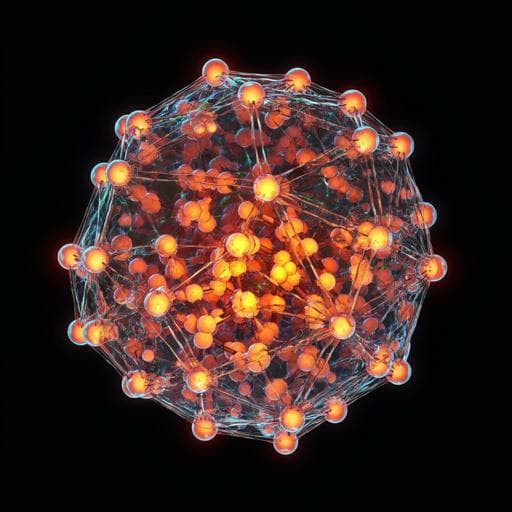
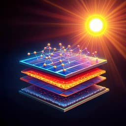
Amazing new research by Bin Wen, Tian Chen, Qixin Yin, Jiangsheng Xie, Chaohua Dai, Ruohao Lin, Sicen Zhou, Jiancan Yu, and Pingqi Gao reveals that treating perovskite surfaces with bidentate ligands significantly enhances solar cell efficiency, achieving an impressive 25.7% efficiency and over 90% efficiency retention after aging. This innovative approach could revolutionize solar technology!

00:00
00:00
~3 min • Beginner • English
Introduction
Metal halide perovskites (ABX3) comprise corner-sharing BX6 octahedra (B = Pb, X = halide) with A-site cations in the cavities. The BX6 framework governs the electronic structure and carrier transport, enabling perovskite solar cells (PSCs) to surpass 26% PCE. However, the PbI6 octahedral network is mechanically and chemically fragile at surfaces and grain boundaries, where defects and ion diffusion are most prevalent. Iodide ions migrate along octahedral edges with low activation energy, are prone to oxidation to I2 by photogenerated holes, and can induce metallic Pb defects, structural collapse, and degradation of transport layers—key barriers to PSC operational stability and commercialization. Prior stabilization strategies have strengthened interactions with A-site cations, enhanced surface bond strength, and introduced low-dimensional capping layers, yet the surface remains soft and susceptible to defect formation and ion migration. This work aims to construct a robust chelated Pb octahedron surface layer on FAPbI3 that suppresses defect generation and iodide migration, reduces nonradiative recombination, and optimizes interfacial energetics for efficient and stable PSCs.
Literature Review
Surface and grain-boundary instabilities dominate perovskite degradation due to high defect densities and ion diffusion. Strategies to mitigate include ammonium salts, small molecules, polymers, and other passivators that reduce defect densities; and low-dimensional perovskites that stabilize surfaces via steric hindrance and PbI6 framework fixation. These approaches improve performance and stability but often leave a soft PbI6 surface susceptible to continued ion migration and degradation. Reviews and key studies highlight ion migration as a central failure mode in PSCs, the role of surface treatments, and the benefits of dimensional engineering and interface optimization. Nonetheless, a need remains for inherently robust surface frameworks that elevate defect formation energies and migration barriers while providing favorable band alignment and passivation.
Methodology
- Synthesis of chelated layer and single crystals: The bidentate ligand N,N'-Dimethyl-1,2-ethanediamine (DMEDA) was reacted with FAPbI3 or PbI2 precursors to form PbI2(DMEDA), evidenced by formation of white precipitates. Single crystals of PbI2(DMEDA) were grown by redissolving precipitates and using an antisolvent vapor-assisted crystallization procedure. - In-situ surface reaction on perovskite: A thin PbI2(DMEDA) layer was formed on FAPbI3 films by dynamically spin-coating DMEDA in isopropanol (IPA) without additional annealing. At high concentration (100 mg mL−1) full films of PbI2(DMEDA) were formed; for surface passivation a lower concentration (1.5 mg mL−1) produced a thin (~5 nm) surface layer. Reactions: (1) FAPbI3 + DMEDA → PbI2(DMEDA) + FAI (dissolved in IPA); (2) PbI2 + DMEDA → PbI2(DMEDA). - Structural and compositional characterization: XRD identified characteristic PbI2(DMEDA) peaks (e.g., ~11.58°) and disappearance of PbI2 (~12.7°) after treatment. XPS detected increased C–C/C–H and C–N (from DMEDA) and reduced FA-related signal, confirming surface conversion. Cross-sectional HRTEM and HAADF-STEM/EDS resolved a compact ~5 nm PbI2(DMEDA) surface layer with slightly lower I and higher N compared with the underlying perovskite. Intrinsic stability of PbI2(DMEDA) powder was tested by XRD after 1000 h at 1 sun and 500 h at 85 °C in air, showing no new impurity phases. - Optoelectronic and interfacial probes: UV–vis and DFT established PbI2(DMEDA) as a wide-gap (~3 eV) direct semiconductor. Steady-state and mapping PL showed enhanced, more uniform emission; TRPL measured increased lifetime. KPFM and UPS determined increased work function and upward band bending at the perovskite surface upon PbI2(DMEDA) formation, implying hole-selective behavior and reduced surface recombination. - Device fabrication: n–i–p PSCs: FTO/SnO2/perovskite (pure FAPbI3)/spiro-OMeTAD/Au with DMEDA IPA (1.5 mg mL−1) spin-coated to form the PbI2(DMEDA) passivation layer. Details: cleaned FTO; SnO2 nanoparticle layer with RbCl additive; FAPbI3 precursor (1.6 M with 20 mol% FAICl in DMF:DMSO 9:1) spin-coated using MACI-IPA antisolvent; annealing; spiro-OMeTAD deposition; Au evaporation. For thermal tests, spiro-OMeTAD was replaced by PTAA. Large-area (1 cm2) devices followed the same flow. HTL-free devices: FTO/SnO2/perovskite/Au. p–i–n PSCs: FTO/NiOx/SAM (Me-4PACz)/perovskite (Cs0.05MA0.1FA0.85PbI3)/C60/BCP/Ag with DMEDA IPA (0.8 mg mL−1) post-treatment. - Device characterization: J–V under AM 1.5 G (100 mW cm−2) with forward/reverse scans; stabilized MPP; EQE and integrated Jsc; unencapsulated MPP stability in air (RH ~20%) and in N2 at ~50 °C; ToF-SIMS depth profiling of iodide distribution after aging; variable-temperature conductivity to extract ion migration activation energy via Nernst–Einstein relation; SCLC in hole-only devices to estimate trap density; PL/TRPL, SEM/AFM, KPFM, UPS/XPS, TEM, XRD as detailed. - DFT calculations: VASP, PBE-GGA, 450 eV cutoff; supercells for FAPbI3, PbI2, and PbI2(DMEDA); iodide vacancy formation energies and iodine migration barriers computed via CI-NEB (6 images) and LBFGS relaxations. Band structure and DOS with 3×3×2 Γ-centered k-point mesh; defect formation energies using standard formalism including chemical potentials, Fermi level, VBM alignment, and finite-size corrections.
Key Findings
- Formation of robust chelated layer: DMEDA coordinates bidentately to Pb2+, displacing two I− and forming a chelated Pb octahedron, yielding a stable PbI2(DMEDA) layer on FAPbI3 via in-situ reaction. XRD, XPS, and TEM confirm a compact ~5 nm surface layer. PbI2(DMEDA) powders show exceptional stability: no impurity phase after 1000 h continuous 1-sun illumination or 500 h at 85 °C in air. - Optoelectronic improvements: PbI2(DMEDA) is a wide-gap (~3 eV) direct semiconductor that passivates and modulates surface energetics. PL intensity and uniformity increase; TRPL lifetime increases from 1.6 µs (control) to 2.6 µs (CPOS). PL peak slightly blue-shifts (812→810 nm), indicating reduced nonradiative recombination. KPFM shows work function increase from 4.4 eV to 4.7 eV; UPS indicates upward band bending favoring hole extraction and electron blocking. - HTL-free device validation: FTO/SnO2/FAPbI3/Au devices show efficiency improvement from 2.2% (control) to 14.3% (CPOS), consistent with a hole-selective, recombination-suppressing surface. - n–i–p device performance: Champion PCE improves from 23.18% to 25.7% (reverse scan), with Voc from 1.136 V to 1.177 V, Jsc from 25.71 to 26.14 mA cm−2, and FF from 79.3% to 83.7%. Stabilized MPP PCE: 23.0% (control) vs 25.5% (CPOS). Certified PCE: 25.04%. EQE-integrated Jsc: 25.23 vs 25.51 mA cm−2 (control vs CPOS). Ideality factor decreases from 1.63 to 1.08, indicating suppressed surface trap-assisted recombination. Trap densities (hole-only SCLC) decrease from 2.27×10^15 to 1.16×10^15 cm−3. 1 cm2 devices reach 23.8% (reverse) and 23.2% (forward). p–i–n devices also show improved Voc, FF, and PCE. - Operational stability: Unencapsulated devices in air (RH ~20%) under 1-sun MPP: CPOS retains >88% after 150 h vs control ~30%. In N2 at ~50 °C under continuous illumination MPP: CPOS retains >90% after ~1000 h, whereas control drops to 80% by 560 h. Thermal stability at 85 °C in N2 (PTAA HTL): CPOS retains 85% after 530 h vs control 56%. - Suppressed iodide migration: ToF-SIMS after MPP aging shows about an order-of-magnitude lower I accumulation in Au and spiro-OMeTAD for CPOS vs control. Temperature-dependent conductivity yields increased I− migration activation energy from 0.35 eV (control) to 0.67 eV (CPOS). DFT: I vacancy formation energy increases from 0.84 eV (FAPbI3) and 1.18 eV (PbI2) to 1.48 eV (PbI2(DMEDA)); migration energy barrier increases to 1.23 eV for PbI2(DMEDA) (vs 0.25 eV in FAPbI3 and 0.39 eV in PbI2).
Discussion
Chelating Pb2+ with the bidentate DMEDA ligand creates a rigidified octahedral framework at the perovskite surface (PbI2(DMEDA)) that is intrinsically stable and energetically unfavorable for iodide vacancy formation and migration. This chelated surface suppresses key degradation pathways—iodide migration to doped HTLs, iodide oxidation to I2, and Pb2+ reduction—thereby preserving interfacial band alignment and transport layer conductivity during operation. Simultaneously, the wide-gap chelate layer reduces surface nonradiative recombination, induces upward band bending, and confers hole selectivity, collectively improving Voc, FF, and stabilized performance. The marked improvements in ion migration activation energy and vacancy formation energy from experiments and DFT rationalize the significant enhancement in operational stability under illumination and heat. These results address core stability limitations of PSCs by hardening the typically soft perovskite surface, offering a generalizable route to passivate and energetically engineer perovskite interfaces.
Conclusion
The study introduces an in-situ formed chelated lead octahedron surface (PbI2(DMEDA)) on FAPbI3 that robustly stabilizes the perovskite surface, suppresses defect formation and iodide migration, and optimizes interfacial energetics. Devices achieve a champion PCE of 25.7% (certified 25.04%), enhanced Voc, Jsc, and FF, and outstanding operational stability (>90% retention after ~1000 h MPP at ~50 °C in N2), with reduced trap densities and substantially higher ion migration activation energy. The chelation-based strategy effectively converts a soft, defect-prone surface into a hard, stable, and hole-selective contact. Future work could explore broader families of multidentate ligands and chelate chemistries, integration with various perovskite compositions and device architectures, and scaling to modules and encapsulated long-term field testing.
Limitations
Listen, Learn & Level Up
Over 10,000 hours of research content in 25+ fields, available in 12+ languages.
No more digging through PDFs, just hit play and absorb the world's latest research in your language, on your time.
listen to research audio papers with researchbunny