Engineering and Technology
Individually addressable and flexible pressure sensor matrixes with ZnO nanotube arrays on graphene
J. Park, R. Ghosh, et al.
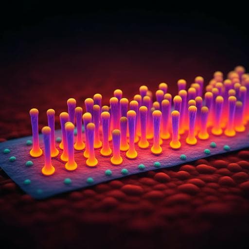
One-dimensional piezoelectric semiconductor nanostructures (nanowires, nanotubes, nanorods) enable compact, high-resolution pressure/force sensor arrays due to their vertical assembly within tiny areas. Among wurtzite piezoelectric semiconductors (ZnO, GaN, AlN, ZnS), 1D ZnO nanostructures have seen extensive use as sensing platforms for artificial intelligence and medical devices via coupling of piezoelectricity with photonics/electronics. For next-generation robotics and human–machine interfaces, tactile sensors require large-scale arrays with high spatial resolution, sensitivity, wide detection range, fast response, and flexibility. Various flexible/stretchable tactile sensors exist based on resistive, capacitive, triboelectric, and piezoelectric mechanisms, each with advantages and drawbacks. Despite advances (including piezo-phototronic sensors and high-resolution devices based on 2D ZnO nanoplatelets), integrating 1D ZnO nanostructures into independently addressable, high-density piezotronic arrays (>1000 dpi) remains challenging due to fabrication complexity. Two-terminal crossbar electrode arrays offer a route to high-density, individually addressable devices, especially when combined with techniques that flip 1D nanostructures to form crossbar contacts. MOVPE/MOCVD enables high-quality, dimension- and position-controlled ZnO nanotube (NT) arrays on graphene, where graphene controls NT dimensions/positions and facilitates lift-off to form efficient crossbar microelectrodes. Leveraging graphene’s mechanical stability, this work fabricates individually addressable, flexible, free-standing vertical ZnO NT pressure/force sensor arrays on graphene, achieving high sensitivity and fast response from single-NT and small bundled arrays, and demonstrating an 8 x 8 addressable matrix with spatial resolution up to 1058 dpi.
- Survey of tactile sensor mechanisms: Resistive sensors (conductive nanomaterials in polymers) offer high sensitivity and simple, low-cost structures but suffer from high power consumption and temperature dependence. Capacitive sensors provide low power consumption, flexibility, high sensitivity, and good spatial resolution but face bulk device structures, dependence on dielectric elastomers, complex measurements, and limited spatial resolution for high-resolution mapping. Triboelectric sensors are self-powered with high sensitivity across forces via differing triboelectric polarities but struggle with dynamic pressure sensing. Piezoelectric sensors offer high sensitivity, fast response, and dynamic pressure detection, with 1D ZnO nanostructures on flexible substrates attracting strong interest for tactile imaging.
- Enhancements via heterostructures, composites, and piezo-phototronics have yielded high spatial resolution, rapid response, and flexibility. Prior work includes high-resolution piezotronic tactile sensors based on 2D ZnO nanoplatelets (e.g., Liu et al.).
- Integration challenges: High-density, individually operated device arrays using vertical 1D nanostructures are difficult to fabricate. Two-terminal crossbar arrays mitigate complexity versus multi-terminal devices. Flipping 1D nanostructures facilitates crossbar contacts at both ends.
- Materials platform: MOVPE/MOCVD growth of position- and dimension-controlled ZnO NT arrays on graphene is established; graphene aids precise NT placement, lift-off for free-standing arrays, and flexible, robust contacts.
Graphene synthesis and transfer: Large-area multilayer graphene was grown on 0.025 mm Cu foil (99.8%) via CVD. Cu was cleaned (acetone, isopropanol), heated to 1030 °C under H2 (100 sccm, 200 Torr), annealed 15 min, then graphene grown 130 min with CH4 (10 sccm) and H2 (100 sccm) at 220 Torr. Samples cooled under H2 at 200 Torr. PMMA was spin-coated; backside graphene was removed by O2 plasma. Cu was dissolved in ammonium persulfate, leaving PMMA-supported graphene, which was transferred to Si/SiO2 (300 nm) substrates and PMMA removed.
Substrate preparation: A 50 nm SiO2 layer was deposited on transferred graphene by PECVD and annealed at 600 °C in O2 to reduce defects. Hole patterns were defined by EBL; SiO2 was dry-etched (CF4 RIE) and then wet-etched (BOE) to remove residual oxide on graphene. Substrates were cleaned (acetone, 2-propanol, nitric acid, DI water).
ZnO nanotube growth by MOVPE/MOCVD: Position-controlled ZnO NT arrays were selectively grown on patterned graphene using a homemade MOCVD system. Precursors: diethylzinc (DEZn, 40 sccm) and O2 (100 sccm); carrier gas Ar (>99.9999%). DEZn bubbler at −10 °C; O2 line isolated to avoid premature reactions. Reactor pressure 3.2 Torr; temperature 690 °C.
Lift-off to form free-standing NTs on graphene: A polyimide (PI, VTEC PI) layer was spin-coated at 4000 rpm and prebaked at 120 °C for 120 s. Oxygen plasma (50 mA, 50 mTorr, 5 min) selectively etched PI at NT tips. The entire layer was mechanically lifted by separating graphene from the SiO2/Si substrate using a Kapton tape frame, leaving NTs suspended with free bottom ends for contact deposition. The free-standing PI layer with ZnO NT/graphene was cured under N2 by rapid thermal annealing (200 °C 3 min; 300 °C 3 min).
Device fabrication (individually addressable arrays and single sensors): The free-standing layer was transferred to a polished, highly doped n-type Si substrate for EBL. Bilayer PMMA (950K/495K) was used for metal liftoff. Top Au electrodes (100 nm) were deposited by e-beam evaporation using a grazing-incidence method: 20° incidence while rotating at 1 rpm to conformally coat the ZnO NT sidewalls and deposit a 100 nm Au layer on PI. The layer was then flipped and transferred onto n-Si to define bottom electrodes (Cr/Au 10/100 nm) on graphene; unprotected backside graphene was etched by O2 plasma, leaving back electrodes beneath graphene strips. Crossbar arrays formed an 8 x 8 matrix of addressable devices. Two crossbar widths were used: 12 µm (3 x 3 NTs) and 20 µm (5 x 5 NTs), with corresponding pixel periodicities: AD12 (pixel 24 x 24 µm²; dot size 12 µm) and AD20 (pixel 40 x 40 µm²; dot size 20 µm). Additionally, two-terminal sensors with single NT, 3 x 3, 5 x 5, and 250 x 250 NTs were fabricated.
Characterization: Morphology examined by FESEM (TESCAN, 30 kV) and SEM (Zeiss AURIGA) at different fabrication stages; the AURIGA system also used for EBL design. TEM (JEOL JEM-2100F) analyzed individual NTs; samples prepared by scratching NTs, dispersing in isopropanol, and drop-casting on lacey-carbon-coated Cu grids (300 mesh). Electrical sensing used I–V and I–T (Keithley 2601) under applied DC bias. Pressure/force application: (i) quasi-static vertical force 0.1–1 kg-wt in 0.1 kg-wt steps with the device affixed to a flat surface and a 1 mm² sapphire spacer to avoid electrical shortcuts; (ii) small pressures from a constant Ar gas flow (MFC), device placed 2 mm from MFC outlet, and for arrays a 45° incidence flow in probe station; for mechanical probing, a third probe with precision knob applied pressure.
- Fabrication of high-quality, dimension- and position-controlled vertical ZnO nanotube arrays on graphene enabled individually addressable, flexible, free-standing pressure/force sensors.
- Device configurations included single NT, 3 x 3, 5 x 5, and 250 x 250 NT arrays, all showing significant pressure/force responses, including to small pressures from inert gas flows.
- An 8 x 8 pixel-addressable matrix with crossbar electrodes was demonstrated; pixel types: AD12 (24 x 24 µm², 12 µm dot) and AD20 (40 x 40 µm², 20 µm dot).
- Spatial resolution reached as high as 1058 dpi for Schottky diode-based sensors composed of ZnO NTs on a flexible substrate.
- Structural metrics: NT diameter ~500 nm; length 9–10 µm; NT wall thickness ~12 nm with interconnected ultrathin inner walls to prevent fracture under pressure; conformal Au coating on NT sidewalls with ~17 nm average thickness near NT tops.
- Contacts: Schottky top contact (ZnO–Au) and ohmic bottom contact (ZnO–graphene–Cr–Au).
- Performance attributes: high sensitivity, fast response, wide detection range, excellent flexibility, and electrical robustness; uniformity and robustness of spatial mapping studied as functions of pixel size, NT count per pixel, and NT lateral dimensions.
By combining MOVPE-grown, dimension- and position-controlled ZnO nanotube arrays with graphene-enabled lift-off and crossbar electrode integration, the study addresses the core challenge of fabricating high-density, individually addressable 1D nanostructure-based tactile sensors. The demonstrated 8 x 8 matrix and two-terminal devices achieve high sensitivity and fast response to both small and larger applied pressures while maintaining flexibility and robustness due to the free-standing architecture and graphene contacts. The Schottky top/ohmic bottom contact scheme enables effective piezoresistive/piezotronic transduction. Achieving up to 1058 dpi spatial resolution highlights the potential for high-resolution tactile imaging. Systematic evaluation across pixel sizes, NT counts, and NT dimensions supports array uniformity and reliable spatial mapping, underscoring relevance to e-skin, human–electronics interfaces, and NEMS/MEMS applications.
The work demonstrates individually addressable, flexible, free-standing pressure/force sensor arrays using vertically aligned ZnO nanotubes on graphene, integrated via crossbar electrodes. Devices ranging from single NT to bundled arrays exhibit high sensitivity, fast response, wide detection range, and mechanical robustness. An 8 x 8 addressable matrix achieves spatial resolution up to 1058 dpi, enabled by Schottky/ohmic contact engineering and precise NT dimension/position control. These results represent an important step toward scalable, high-resolution tactile sensors applicable to wearable electronics, smart skin, robotics, and healthcare, opening opportunities for advanced human–electronics interfaces and NEMS/MEMS integration.
Related Publications
Explore these studies to deepen your understanding of the subject.