High-performance piezoelectric energy harvesting in amorphous perovskite thin films deposited directly on a plastic substrate
J. Han, S. H. Park, et al.
Explore these studies to deepen your understanding
Adjacent work that informs or extends this paper's methodology and findings.

Multifunctional electrochromic energy storage devices by chemical cross-linking: impact of a WO3·H2O nanoparticle-embedded chitosan thin film on amorphous WO3 films
B. Koo, M. Jo, et al.
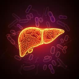
Consumption of a high energy density diet triggers microbiota dysbiosis, hepatic lipidosis, and microglia activation in the nucleus of the solitary tract in rats
D. M. Minaya, A. Turlej, et al.

Unveiling the origins of non-performance-oriented behavior in China's local governments: a game theory perspective on the performance-based promotion system
H. Shang, H. Liu, et al.

The influence of blue light on sleep, performance and wellbeing in young adults: A systematic review
M. I. Silvani, R. Werder, et al.


