
Engineering and TechnologyNature Communications
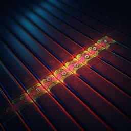
Femtosecond pulse amplification on a chip
M. A. Gaafar, M. Ludwig, et al.
Discover how a team of researchers has achieved over 50-fold amplification of femtosecond pulses in a CMOS-compatible photonic chip, reaching an impressive 800 W peak power. This breakthrough could pave the way for chip-integrated femtosecond technology that rivals traditional tabletop sources.
Related Publications
Explore these studies to deepen your understanding
Adjacent work that informs or extends this paper's methodology and findings.

Engineering and Technology
Bright and dark Talbot pulse trains on a chip
J. Wu, M. Clementi, et al.
Engineering and Technology
Design and fabrication of a vigorous “cavitation-on-a-chip” device with a multiple microchannel configuration
F. R. Talabazar, M. Jafarpour, et al.

Medicine and Health
Development of a novel testis-on-a-chip that demonstrates reciprocal crosstalk between Sertoli and Leydig cells in testicular tissue
S. Park, M. G. Kook, et al.
Engineering and Technology
A mid-infrared lab-on-a-chip for dynamic reaction monitoring
B. Hinkov, F. Pilat, et al.


