
Engineering and Technology
Enhanced charge carrier transport and defects mitigation of passivation layer for efficient perovskite solar cells
Z. Qu, Y. Zhao, et al.
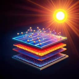
Discover how a groundbreaking binary and synergistic post-treatment method enhanced the passivation layers in perovskite solar cells, achieving a stunning power conversion efficiency of 26.0%. This research, conducted by Zihan Qu and colleagues, offers exciting advancements in solar cell technology.
~3 min • Beginner • English
Introduction
Perovskite solar cells (PSCs) have rapidly advanced over the last decade, reaching certified power conversion efficiencies (PCEs) near 26%, rivaling crystalline silicon. Among performance-boosting strategies—composition engineering, crystal growth modulation, and surface passivation—passivation is crucial for suppressing nonradiative recombination and lowering trap densities. Yet, many conventional passivation agents (2D perovskites, inorganic compounds, polymers, bulky organic salts) are poorly conductive, which hampers interfacial charge transport and limits improvements in fill factor (FF) relative to short-circuit current density (Jsc) and open-circuit voltage (Voc). The study addresses the central challenge of simultaneously achieving strong defect passivation and efficient charge transport at the perovskite surface. The hypothesis is that a binary synergistic post-treatment (BSPT) using mixed organic iodide salts can yield a crystalline, ordered, and energetically well-aligned passivation layer that enhances hole extraction/transport while further reducing surface defects, thereby increasing FF and overall PCE.
Literature Review
Previous work has shown surface passivation to be effective in reducing defect densities and nonradiative recombination in PSCs, including the use of bulky organic ammonium iodides such as phenethylammonium iodide (PEAI), 2D perovskites, inorganic passivants, and polymers. However, these materials typically exhibit low conductivity, which can impede charge transfer even with ultrathin layers and contribute to lagging FF relative to the Shockley–Queisser limit. Alternative strategies have explored semiconducting polymer passivants with flat-band alignment enabling high FF (~83%) and engineered passivation layer distributions (e.g., nanopatterned electron transport layers) achieving FF ~83.9%. Combined-passivant approaches have been reported mainly focusing on reducing nonradiative losses via defect density reduction. Building on this context, the present work investigates a mixed organic halide system (PPAI + tBBAI) aiming not only at defect mitigation but also at improving passivation-layer crystallinity, molecular packing, energy alignment, and hence charge transport.
Methodology
- Materials and device structure: Planar n–i–p PSCs with architecture FTO/SnO2/perovskite/passivation layer/Spiro-OMeTAD/Au. Active perovskite: RbCl-doped FAPbI3 (two-step deposition).
- Binary synergistic post-treatment (BSPT): 4-tert-butylphenylmethylammonium iodide (tBBAI) blended with phenylpropylammonium iodide (PPAI) in isopropanol (IPA). Optimal concentrations: 10 mg/mL PPAI + 10 mg/mL tBBAI. The solution was spin-coated on the perovskite film at 5000 rpm without annealing. Control used unary PPAI (10 mg/mL). Variations of tBBAI (5–15 mg/mL) were screened.
- Perovskite deposition: PbI2 (1.5 M) with 5 mol% RbCl in DMF:DMSO (9:1), spin-coated and pre-annealed; then FAI:MACl in IPA spin-coated to form precursor, followed by annealing at 150 °C for 15 min at 30–40% RH to obtain α-FAPbI3.
- HTL deposition: Spiro-OMeTAD with Li-TFSI/tBP/FK209 dopants in chlorobenzene (72.3 mg/mL), spin-coated; overnight oxidation (25 °C, 1% RH). For thermal stability tests, PTAA:TPFB (40 mg/mL; 10:1.5 wt ratio) replaced Spiro-OMeTAD.
- Electrode: 80 nm Au thermally evaporated. Active area defined by 0.07461 cm2 mask; device area 0.108 cm2.
- Structural and surface characterization: GIXRD, conventional XRD, GIWAXS (SSRF BL17B1), XPS, UPS, SEM, AFM, KPFM, UV–Vis, ssPL, TRPL, PLQY, PL mapping, transient reflection spectroscopy (TRS).
- Electrical/device characterization: J–V under AM 1.5G (100 mW cm−2), EQE, dark I–V, series resistance, MPP tracking (unencapsulated, N2, 50 ±5 °C), light-intensity dependent Voc and Jsc, Mott–Schottky (C–V) for Vbi, thermal admittance spectroscopy (TAS) for trap density of states (tDOS), electrical impedance spectroscopy (EIS), transient photocurrent (TPC), open-circuit voltage decay (OCVD), photo-CELIV for mobility.
- All-atom molecular dynamics (AA-MD): GROMACS with OPLS-AA. Systems of PPAI-only and PPAI+tBBAI in IPA; solvent removal to emulate film formation. Analyses: radial distribution function (RDF), interaction energies, molecular conformation/orientation distributions.
Key Findings
- Passivation layer crystallinity and packing:
- GIXRD: New low-angle diffraction peaks indicate passivation layer formation; PPAI at 4.76°, tBBAI at 4.42°, BSPT at 4.55°, consistent with Vegard’s law, evidencing full fusion and enhanced crystallinity in BSPT.
- GIWAXS: Stronger Bragg spots along qz for BSPT (q ≈ 3.24 nm−1 vs 3.39 nm−1 for PPAI), indicating more parallel molecular orientation and ordered packing conducive to vertical charge transport.
- XPS: Stronger C–C/π–π signals and highest Pb:I ratio for BSPT, indicating better passivator coverage and iodine-vacancy filling.
- AA-MD: Higher RDF first-peak intensity for PPAI–tBBAI pairs vs PPAI–PPAI; stronger PPAI–tBBAI interaction energy than PPAI–PPAI; denser packing and slightly increased benzene-plane/tail angle (~75.4°) in blends.
- Energy alignment and surface potential:
- UPS work function shift: pristine −4.67 eV → PPAI −4.23 eV → BSPT −3.45 eV; induces dipole accelerating hole transport and blocking electrons.
- BSPT provides an intermediate HOMO level and much smaller HOMO offset to Spiro-OMeTAD (0.13 eV) vs PPAI (0.65 eV), favoring hole extraction.
- KPFM: Flatter CPD distribution and higher average CPD with BSPT, indicating improved interfacial contact and alignment.
- Morphology and coverage:
- SEM/AFM: PPAI leaves local aggregates and pinholes; BSPT yields uniform coverage and smoother surface (Ra: pristine 22.7 nm; PPAI 17.8 nm; BSPT 9.76 nm), reducing leakage paths.
- Defect passivation and recombination:
- ssPL/PLQY: BSPT shows ~2× ssPL vs PPAI and > pristine, indicating fewer surface traps.
- TRPL lifetimes: pristine 0.81 µs; PPAI 3.46 µs; BSPT 6.36 µs (fewer recombination centers).
- TRS (700 nm pump): BSPT exhibits slower surface carrier decay, indicating reduced surface recombination.
- PL mapping: BSPT shows more uniform and stronger PL across 15 × 15 µm area.
- TAS tDOS (deep traps >0.4 eV): peak reduced from 1.84 × 10^17 to 7.3 × 10^16 cm−3 eV−1 with BSPT.
- EIS: Larger recombination resistance after BSPT.
- Device metrics and operation:
- Statistical improvement driven primarily by FF with reduced series resistance; slight Voc increase (~0.01 V) from already high control (~1.18 V); Jsc unchanged.
- Champion lab device: PCE 26.75% (negligible hysteresis); steady power output 26.1% for 600 s at 1.04 V.
- Certified (JET): quasi-stabilized PCE 26.0% with Voc 1.19 V, Jsc 26.00 mA cm−2, FF 84%; ratios to S–Q limit: 83.4% (Voc), 95% (Jsc), 94.1% (FF), 93.2% (PCE). Listed by NREL and Green et al.
- Stability (unencapsulated, N2, 50 ±5 °C): BSPT retains 81% of initial PCE after 450 h MPP (control 78%).
- Light-intensity Voc: Ideality factor 1.09 (BSPT) vs 1.26 (control), indicating suppressed SRH recombination.
- Mott–Schottky: Vbi increased from 1.00 V to 1.04 V with BSPT.
- Dark I–V: Lower leakage near 0 V, faster current rise at forward bias for BSPT (better transport).
- TPC: Faster photocurrent decay for BSPT; lifetime ~0.94 µs (faster extraction).
- OCVD: Slower Voc decay for BSPT (more balanced transport).
- Photo-CELIV mobility: 2.05 × 10^−3 vs 1.90 × 10^−3 cm^2 V^−1 s^−1 (BSPT vs control).
- Overall: BSPT enhances passivation-layer crystallinity/ordering and aligns energy levels to improve hole extraction/transport while further reducing defects, yielding record efficiency and robust operational stability.
Discussion
The study demonstrates that combining PPAI with tBBAI in a binary synergistic post-treatment overcomes the traditional trade-off between strong surface passivation and efficient charge transport. Enhanced crystallinity and ordered molecular orientation/packing in the BSPT layer establish better-connected charge transport pathways, while UPS/KPFM show favorable energy level alignment and uniform surface potential for accelerated hole extraction and electron blocking. Spectroscopic probes (ssPL, TRPL, TRS) and TAS/EIS confirm reduced trap densities and suppressed SRH recombination. Device-level analyses (light-intensity Voc, Mott–Schottky, dark I–V, TPC, OCVD, photo-CELIV) corroborate improved charge separation, reduced leakage, faster extraction, balanced transport, and slightly higher built-in potential. These interfacial improvements primarily boost FF, with a modest Voc gain and stable Jsc, culminating in a certified 26.0% PCE and superior PCE-to-SQ ratios. The findings provide a path to tailor passivation layers that both passivate defects and actively facilitate carrier transport, with implications for other perovskite optoelectronic devices.
Conclusion
A binary synergistic post-treatment (BSPT) using mixed organic iodide salts (PPAI + tBBAI) forms a crystalline, well-packed, and energetically aligned passivation layer on FAPbI3 that simultaneously enhances carrier transport and suppresses defects. This approach improves hole extraction/transfer, reduces SRH recombination, lowers deep-trap density, and smooths/fully covers the perovskite surface. The resulting n–i–p PSCs deliver a certified quasi-stabilized PCE of 26.0% (Voc 1.19 V, Jsc 26.00 mA cm−2, FF 84%) and retain 81% of initial PCE after 450 h MPP tracking. Future work should target operational durability by: developing more stable HTLs to replace Spiro-OMeTAD, engineering interlayers to suppress ion migration, exploring more thermally robust passivation agents, and improving encapsulation and UV filtering. The BSPT concept is broadly applicable to perovskite interfaces in photovoltaics and other optoelectronics.
Limitations
- Operational stability of normal (n–i–p) devices with Spiro-OMeTAD remains below commercial requirements; degradation to ~81% of initial PCE after 450 h MPP without encapsulation.
- Thermal stability tests show rapid early degradation (first ~50 h) attributed to low-dimensional perovskite formation on the surface; indicates the need for more thermally stable passivants.
- Use of organic functional layers (passivation and HTL) can limit long-term robustness; inorganic replacements or stabilized formulations may be necessary.
- Environmental (humidity/UV) stability remains a concern; requires improved encapsulation and UV filtering.
- The AA-MD simulations used higher solute concentrations than experiments due to computational limits, which may not capture all kinetic details of film formation.
Related Publications
Explore these studies to deepen your understanding of the subject.