
Engineering and Technologynpj 2D Materials and Applications
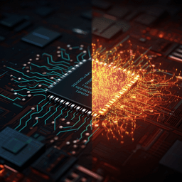
Electron-beam-irradiated rhenium disulfide memristors with low variability for neuromorphic computing
S. Li, B. Li, et al.
Discover the groundbreaking potential of a two-terminal lateral memristor using electron-beam-irradiated rhenium disulfide (ReS2), showcasing stable and gradual resistive switching. This innovative research by Sifan Li, Bochang Li, Xuewei Feng, Li Chen, Yesheng Li, Li Huang, Xuanyao Fong, and Kah-Wee Ang paves the way for energy-efficient neuromorphic computing through Schottky barrier height modulation.
Related Publications
Explore these studies to deepen your understanding
Adjacent work that informs or extends this paper's methodology and findings.

Engineering and Technology
Graphene-based 3D XNOR-VRRAM with ternary precision for neuromorphic computing
B. Alimkhanuly, J. Sohn, et al.

Engineering and Technology
Toward grouped-reservoir computing: organic neuromorphic vertical transistor with distributed reservoir states for efficient recognition and prediction
C. Gao, D. Liu, et al.

Engineering and Technology
Transistors with ferroelectric ZrxAl₁₋ₓOY crystallized by ZnO growth for multi-level memory and neuromorphic computing
M. M. Islam, A. Ali, et al.
Computer Science
Spike-based dynamic computing with asynchronous sensing-computing neuromorphic chip
M. Yao, O. Richter, et al.


