
Electrodeposition of ternary compounds for novel PV application and optimisation of electrodeposited CdMnTe thin-films
A. E. Alam, O. I. Olusola, et al.
Explore these studies to deepen your understanding
Adjacent work that informs or extends this paper's methodology and findings.

Application of chemometrics for modeling and optimization of ultrasound-assisted dispersive liquid–liquid microextraction for the simultaneous determination of dyes
S. Shojaei, S. Shojaei, et al.
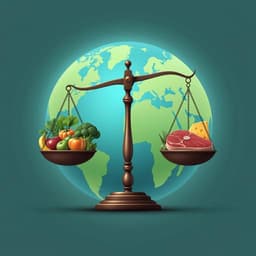
Developing a novel optimisation approach for keeping heterogeneous diets healthy and within planetary boundaries for climate change
P. E. Colombo, L. S. Elinder, et al.
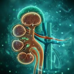
Novel Biomarkers for Early Detection of Acute Kidney Injury and Prediction of Long-Term Kidney Function Decline after Partial Nephrectomy
M. Allinovi, F. Sessa, et al.

A Multicenter Randomized Controlled Trial of Microbiome-Based Artificial Intelligence-Assisted Personalized Diet vs Low-Fermentable Oligosaccharides, Disaccharides, Monosaccharides, and Polyols Diet: A Novel Approach for the Management of Irritable Bowel Syndrome
V. Tunali, N. Ç. Arslan, et al.


