Engineering and Technology
A customizable, low-power, wireless, embedded sensing platform for resistive nanoscale sensors
S. Nedelcu, K. Thodkar, et al.
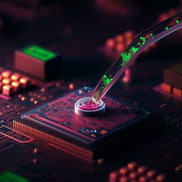
The study addresses the need for portable, low-power, and customizable gas sensing platforms to improve air quality monitoring beyond stationary, costly, and maintenance-intensive conventional systems (e.g., gas chromatography). Motivated by public health concerns (e.g., WHO-estimated seven million premature deaths annually due to poor air quality) and regulatory limits for NO₂ (EU hourly and annual limits; US EPA standards), the authors aim to develop an embedded, IoT-compatible platform capable of interfacing high-sensitivity resistive nanosensors. The work situates itself among prior IoT-based air monitoring solutions and commercial sensors, noting trade-offs in power, size, configurability, and data handling (e.g., limited resolution, lack of wireless or local storage). It also builds on advances in nanomaterial-based sensors (nanowires, graphene, CNTs, MOx) while acknowledging challenges such as device variation and long-term stability. The purpose is to deliver a reprogrammable, low-power, wireless platform with high dynamic range and precision suitable for nanoscale resistive sensors and compliant with environmental monitoring needs.
The paper reviews several commercial and research sensing solutions: a multi-gas portable PCB system using off-the-shelf sensors requiring 11–24 V and 2.5–6 W with 8-bit output and no local storage or wireless; a compact CO₂ module (5 V, 20–200 mA, 5 s updates) with proprietary self-calibration but lacking reprogrammability and embedded wireless; and a wearable multi-pollutant platform employing neural-network calibration, drawing 50 mA with two sensors. Another system for CO, SO₂, and NO₂ offers 16-bit resolution and BLE at ~150 mW average but does not fully exploit custom readout or calibration. The authors contrast these with their goals of software-driven configurability, low power, higher resolution, and integrated wireless/data logging. The review summarizes nanomaterials used in gas sensing (nanowires, graphene and its derivatives/composites, CNTs, MOx composites) and cites prior CNT and nanowire-based systems, noting that some prior NO₂ CNT sensors had ppm-level detection, above EU ppb-level needs. Persistent challenges include device variability and ON-current degradation over time.
Hardware architecture: The platform centers on an ATmega2560 microcontroller with flexible timers/counters, SPI, serial port, and power-saving modes (~3 mW at 1 MHz active). Local data storage is via an SD card over SPI. Wireless communication is provided by a BLE module, selected for favorable data rate versus power (~10 mA) compared with Wi‑Fi (~300 mA) and LoRa (~120 mA). A sealed on-board test chamber with gas inlet/outlet allows controlled exposures.
Sensor Bias Block (SBB): Sensor biasing is software-defined and generated by three dual-channel 12-bit DACs (MCP4922), providing 0–5 V outputs (Vbias1–Vbias4) with 1.25 mV resolution. A two-stage inverting charge pump (two MAX660 in cascade) and an op-amp with R/2R scaling create a bipolar Vbias5 spanning −10 V to +5 V with 3.65 mV resolution, enabling bias schemes including elevated self-heating.
Sensor Signal Acquisition (SSA): Nanosensor currents are digitized using a multichannel current-to-digital converter (CDC), DDC114, which employs time-interleaved discrete-time integrators followed by ADCs with configurable 16- or 20-bit resolution. The full-scale (FS) input current range is programmable by integration time (Tconv) and selectable integrator capacitance (Crange from an integrated capacitor bank of 3, 12.5, 25, 50 pF), controlled via three digital signals (eight combinations). An external microcontroller timer provides precise CDC timing via interrupts. Sampling rate is tunable from 0.001 to 3.125 kSPS by setting Tconv in approximately 2000 to 0.64 ms range. Overall, the platform supports FS current ranges from 1.5 nA to 7.2 µA.
Control and automation: An event-triggered finite state machine (FSM) on the microcontroller orchestrates bias programming, CDC configuration, data logging to SD, and BLE transmission. Experiment protocols are defined in a CSV (Stimuli.CSV) stored on the SD card, specifying voltage levels and timing; resulting measurements are saved to Results.CSV. The FSM states include power-save/idle and high/medium/low power operations, with transitions driven by internal/external interrupts and timing.
Characterization procedures: The authors evaluated platform bandwidth via Tconv settings, input-referred RMS current noise and offset with inputs open (including PCB/socket/package parasitics), and verified bias waveforms using staircase stimuli defined in Stimuli.CSV. The BLE interface was used to visualize real-time sensor bias levels. A CNT nanosensor in a sealed chamber was exposed to NO₂ from 200 ppb down to 1 ppb to demonstrate sensing capability.
- Measurement capability: Current acquisition full-scale range from 1.5 nA to 7.2 µA with up to 20-bit resolution; sampling rates up to 3.125 kSPS.
- Biasing: Programmable unipolar 0–5 V (1.25 mV resolution) and bipolar −10 V to +5 V (3.65 mV resolution) sensor biases, enabling dynamic bias schemes including self-heating.
- Control and data handling: FSM-driven automated operation with user-defined CSV protocols; on-board SD logging and BLE transmission.
- Power: Average power consumption of 64.5 mW for a protocol with three samples per second, including BLE advertisement at 0 dBm.
- Noise/offset: With four CDC input channels open, input-referred RMS current noise measured around 1.11–1.17 nA with offsets approximately −0.09 to +0.98 nA (channel-dependent), indicating low noise floor considering full-scale ranges.
- Bandwidth tuning: Front-end integrator bandwidth adjustable via Tconv; transfer function derived and tunable frequency response demonstrated.
- Physical integration: 95 mm × 65 mm PCB integrates BLE, microcontroller, SD card, and a sealed gas test chamber.
- Demonstration: CNT nanosensor exposure to NO₂ from 200 ppb down to 1 ppb showed measurable signals at 1 ppb. The 3σ limit of detection was 23 ppb (1σ: 7 ppb) in slope detection mode, accounting for variations across repeated measurements.
- Applicability: The platform’s wide current range and configurability are suited to resistive nanosensors such as silicon nanowires, CNTs, graphene, and other 2D materials, supporting IoT deployment.
The results demonstrate that a low-power, reprogrammable, wireless embedded platform can reliably interface with high-sensitivity resistive nanosensors while providing precise current measurement over orders of magnitude and flexible, software-defined biasing. The combination of a configurable CDC, programmable biasing (including bipolar supply), and an FSM enabling custom measurement protocols addresses key limitations of many commercial systems (fixed functionality, higher power, limited resolution, lack of wireless/local storage). The verified noise and offset levels, along with tunable bandwidth, support high-precision sensing across different operating regimes. The CNT NO₂ sensing demonstration confirms that the platform can capture ppb-level responses and achieve a 3σ LOD of 23 ppb in a realistic protocol including repeatability variations, aligning the system’s performance with regulatory monitoring needs more closely than ppm-level prior devices. Together, these findings validate the platform as a versatile foundation for environmental sensing within IoT ecosystems and as a tool for exploring and calibrating diverse resistive nanosensors.
The paper presents a customizable, battery-operated, wireless embedded platform for nanoscale resistive sensors featuring: (i) wide current acquisition range (1.5 nA–7.2 µA) at up to 20-bit resolution and variable sampling up to 3.125 kSPS; (ii) programmable unipolar/bipolar biasing (0–5 V and −10 to +5 V) with fine resolution; (iii) an FSM enabling flexible, CSV-defined measurement routines; and (iv) integrated SD logging and BLE communication with low average power (~64.5 mW at 3 samples/s with BLE advertising). A state-of-the-art CNT NO₂ sensing demonstration achieved signals down to 1 ppb and a 3σ LOD of 23 ppb. These capabilities make the platform broadly applicable to resistive nanosensors (e.g., nanowires, CNTs, graphene and 2D materials) in IoT contexts. Potential future work includes implementation of automated calibration procedures, multi-sensor operation via CDC daisy-chaining, and extended field deployments to assess long-term stability and variability.
Explicit limitations of the platform are not extensively detailed; however, the authors note broader challenges for nanosensor transducers such as device-to-device variation and ON-current degradation over time, which can affect measurement stability and calibration needs. The demonstrated NO₂ sensing achieved measurable responses at 1 ppb but a 3σ LOD of 23 ppb when accounting for variability, indicating that noise, drift, and repeatability influence ultimate detection limits. Parasitic capacitances and leakage from PCB, sockets, and packages contribute to input noise/offset, which were characterized but remain practical constraints.
Related Publications
Explore these studies to deepen your understanding of the subject.

