Engineering and TechnologyNature Communications
Ubiquitous organic molecule-based free-standing nanowires with ultra-high aspect ratios
K. Kamiya, K. Kayama, et al.
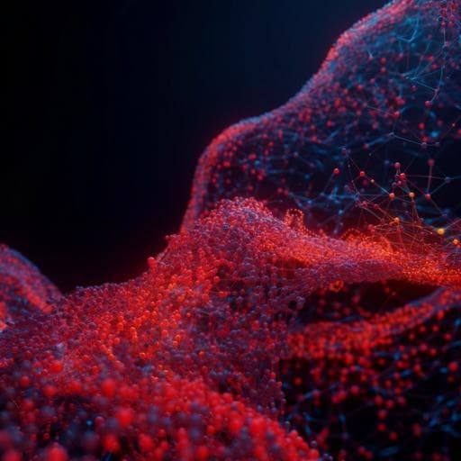
Discover groundbreaking research by Koshi Kamiya and colleagues from Kyoto University and the Takasaki Advanced Radiation Research Institute, where a novel technique using high-energy charged particles has led to the production of free-standing 1D organic nanostructures with incredibly high aspect ratios. This innovative approach promises significant advancements in semiconductor device integration and functionality.
Related Publications
Explore these studies to deepen your understanding
Adjacent work that informs or extends this paper's methodology and findings.
Chemistry
A high mobility air-stable n-type organic small molecule semiconductor with high UV-visible-to-NIR photoresponse
Y. Guan, J. Qiao, et al.

Engineering and Technology
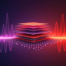
Moderate-coherence sensing with optical cavities: ultra-high accuracy meets ultra-high measurement bandwidth and range
J. Dickmann, L. S. Neto, et al.
Medicine and Health
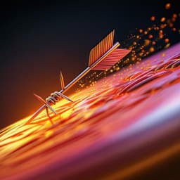
Barbed arrow-like structure membrane with ultra-high rectification coefficient enables ultra-fast, highly-sensitive lateral-flow assay of cTnI
J. Li, Y. Liu, et al.

Engineering and Technology
Nanotransistor-based gas sensing with record-high sensitivity enabled by electron trapping effect in nanoparticles
Q. Hu, P. Solomon, et al.


