PhysicsNature Communications
Spin defects in hBN as promising temperature, pressure and magnetic field quantum sensors
A. Gottscholl, M. Diez, et al.
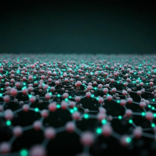
This groundbreaking research by authors including Andreas Gottscholl and Matthias Diez reveals how negatively charged boron vacancies in hexagonal boron nitride can serve as atomic-scale sensors for measuring temperature, magnetic fields, and pressure. The findings highlight the impressive sensitivity of these intrinsic sensors in 2D material heterostructures.
Related Publications
Explore these studies to deepen your understanding
Adjacent work that informs or extends this paper's methodology and findings.
Physics
Drastic enhancement of magnetic critical temperature and amorphization in topological magnet EuSn₂P₂ under pressure
W. Bi, T. Culverhouse, et al.

Physics
Photoexcitation induced magnetic phase transition and spin dynamics in antiferromagnetic MnPS<sub>3</sub> monolayer
Y. Gao, X. Jiang, et al.

Physics
Intersystem crossing and exciton-defect coupling of spin defects in hexagonal boron nitride
T. J. Smart, K. Li, et al.
Physics
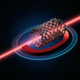
Nanotube spin defects for omnidirectional magnetic field sensing
X. Gao, S. Vaidya, et al.


