Engineering and Technology
Programmed multimaterial assembly by synergized 3D printing and freeform laser induction
B. Zheng, Y. Xie, et al.
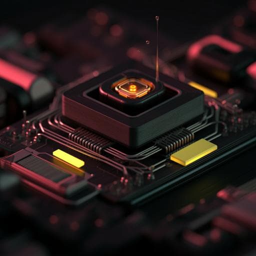
The study addresses the challenge of assembling diverse structural and functional materials into complex, multifunctional 3D objects with precise spatial placement of functional elements. Existing multimaterial fabrication methods (embedded printing, transfer printing, multimaterial 3D printing, DLP, and multi-axis extrusion) face limitations in geometry complexity, placement precision, materials compatibility, and wasteful, multi-step processes. The authors propose FMAP, a synergistic platform that integrates fused filament fabrication (FFF), direct ink writing (DIW), and freeform laser induction (FLI) to enable programmed placement and in-situ synthesis/patterning of functional materials (e.g., LIG, metals, metal oxides) within or on 3D printed structures. The goal is to realize integrated 3D devices with high materials utilization, reduced processing steps, and broader materials options.
Prior multimaterial approaches include embedded 3D printing for soft electronics and strain sensors; multi-nozzle/core–shell DIW for diverse and core–shell structures; multi-axis FFF and conformal DIW for depositing conductive traces on curved surfaces; and DLP for multimaterial photopolymers. However, embedded printing requires molds and struggles with hollow/freestanding features; core–shell methods co-extrude materials continuously, limiting selective placement (e.g., outer surfaces); DIW composites often compromise electrical conductivity/mechanical strength; and DLP is restricted to photosensitive resins with inefficient vat switching and material purging. Direct laser writing (DLW) expands materials choices (LIG, metals, oxides, semiconductors, ceramics) but is largely confined to 2D patterning. A recent 5-axis FLI method enables conformable electronics on freeform surfaces, yet spatial patterning within 3D structures remained challenging. These gaps motivate a more versatile, integrated methodology.
FMAP integrates three processes on a single 5-DOF platform: (1) FFF builds structural components from thermoplastics (PC, PETG, TPU, PVDF). (2) FLI (450 nm, up to 5 W) converts selected regions to functional materials: it induces laser-induced graphene (LIG) from suitable polymers (e.g., PC) and converts DIW-deposited precursors into metals/oxides (Ag, Fe, Co, Ni, CuO), forming LIG-based composites (e.g., LIG/Ag). (3) DIW deposits inks/precursors (e.g., silver citrate, lignin/silver mixtures) onto prepatterned LIG or printed substrates. For non-laser-convertible polymers (TPU, PETG), lignin/silver inks are DIW-deposited and immediately laser-converted to LIG/Ag; the heated build plate (100 °C) accelerates solvent evaporation. The tool head hosts an FFF hotend, a DIW nozzle, and a laser module; coordinated motion enables conformal patterning across complex geometries while avoiding cross-contamination by rotating end effectors. Workflow example (3D wireless LED): print PC layers by FFF; FLI converts selected PC to LIG; DIW deposits Ag precursor on LIG; FLI converts to LIG/Ag to form high-conductivity electrodes; subsequent FFF encapsulates traces; LEDs are integrated. The same approach enables functional elements inside or on surfaces of 3D objects. Characterization included SEM/EDS for compositional mapping of LIG/metal(oxide) composites, Raman spectroscopy for graphitic quality, tensile testing of LIG-embedded PC, electrical measurements of sheet resistance and device performance, IR thermography and COMSOL FEA for microfluidic Joule heating, and Hall sensing for electromagnet response. Applications fabricated included: a 5×5 LED crossbar circuit with multilayer LIG/Ag electrodes; self-capacitive touchpads and sliders (rigid and flexible TPU); a ZnO UV sensor integrated with NE555 oscillator; a PC helical spring and robotic gripper with embedded LIG strain sensors; a multilayer Ag-coil/Fe-core micro-electromagnet; and a microfluidic reactor with an embedded LIG Joule heater for ZIF-8 synthesis.
- FMAP platform: 5-DOF motion with integrated FFF, DIW, and 450 nm/5 W laser for FLI enables selective, conformal patterning within 3D structures; near-100% materials utilization for patterned conductors compared to etching-based PCB workflows.
- Materials and resolution: Conductive LIG traces as narrow as 200 µm can power LEDs; best laser-induced silver linewidth ~100 µm (precursor and laser-dependent). LIG thickness increases with laser power.
- Mechanical integrity: PC specimens with embedded LIG (various LIG dimensions, PC layer heights 0.1–0.2 mm) maintained tensile strengths >35 MPa, comparable to pure PC; increasing LIG thickness/width decreased tensile strength and fracture strain.
- Electrical properties: LIG/Ag sheet resistance down to 12.36 Ω/sq at 2.5 W laser power; LIG alone much higher (kΩ/sq scale). Raman of LIG shows D, G, 2D peaks with I_D/I_G ~1.5 and graphitic domain sizes >60 nm at 2.5 W.
- Complex 3D structures: Demonstrated gyroid, Schwarz surfaces, helix, gears, fans, and embedded/surface LIG patterns in complex 3D prints.
- 5×5 LED crossbar: Multilayer LIG/Ag electrodes embedded/encapsulated by FFF; individually addressable LEDs display patterns (e.g., “HELLO”).
- Self-capacitive touch interfaces: 9-electrode touchpad (rigid PETG and flexible TPU) shows >20% capacitance change on touched electrodes with negligible cross-talk; BLE control of LED arrays. Slider with two triangular electrodes exhibits linear position response; performance retains high sensitivity with curvature increase (capacitance change decreases slightly from 73.4% to 66.6% as curvature rises 0 to 2.75).
- UV sensor (ZnO): Photocurrent I vs UV intensity P follows ln(I) = 0.98 ln(P) − 25.3 (R² = 0.99). LED blink frequency f = 3.9×10^-3 P + 0.18 (R² = 0.99) under NE555 oscillator circuit.
- LIG-embedded spring/gripper: Spring’s relative resistance change ΔR linear with displacement D: ΔR = 2.6×10^-3 D − 1.7×10^-3 (R² = 0.98). Stable after 640 cycles at 3 mm displacement, indicating durability; gripper senses force for closed-loop manipulation.
- Micro-electromagnet: Laser-induced 4-layer Ag coil with Fe core encapsulated in PETG; Hall sensor detects on/off within 0.2–0.5 s. Measured rotation speeds derived from voltage spikes match motor inputs across 20–200 rpm with R² ≈ 1.0.
- Microfluidic reactor with LIG heater: Channel temperatures reach ~101 °C without flow; at 30 V/0.1 A, temperatures decrease with increasing flow rate (66.4 °C at 4.5 µL/s to 57.9 °C at 18 µL/s), consistent with FEA. Elevated-temperature synthesis yields ZIF-8 nanoparticles (~200 nm) with strong UV–Vis absorbance and sharp XRD peaks at 2θ = 7.2°, 10.2°, 12.6°, 14.6°, 16.3°, 17.9°, indicating high crystallinity.
The FMAP approach directly addresses limitations in existing multimaterial fabrication by decoupling structural printing from functional material synthesis and by enabling precise spatial patterning inside or on complex 3D geometries. By unifying FFF, DIW, and FLI on a single, coordinated platform, FMAP reduces process steps, boosts materials utilization (near-100% for conductive features), and broadens the materials palette beyond photosensitive resins or composite inks of limited performance. Demonstrations across electronics, sensors, HMI, robotics, and microfluidics validate FMAP’s versatility. Devices exhibited high linearity and sensitivity (e.g., UV sensor R² = 0.99, spring R² = 0.98, electromagnet speed sensing R² ≈ 1.0), robust mechanical integrity (>35 MPa tensile in LIG-embedded PC), and fine patterning (~100–200 µm), supporting reliable performance in real 3D environments. This integrated methodology enables embedded and conformal functionalization without lithography or transfer, highlighting significant implications for scalable, sustainable fabrication of multifunctional 3D engineered systems.
This work introduces FMAP, a synergized platform combining FFF, DIW, and FLI for programmed assembly of structural and functional materials within complex 3D objects. The method achieves precise, conformal, and embedded patterning of LIG and laser-induced metals/oxides, enabling integrated devices such as LED crossbar arrays, capacitive touch interfaces and sliders, UV sensors, LIG-embedded springs and haptic grippers, micro-electromagnets, and microfluidic reactors with in-situ Joule heating for nanoparticle synthesis. The approach offers high materials utilization, minimal waste, and versatility across materials and geometries. Future work will target higher throughput via parallelized end-effectors, improved resolution with advanced laser optics, and expansion to broader applications (e.g., robotics) and processes (e.g., aerosol printing) to further extend the materials and device capabilities.
Current limitations include sequential operation of FFF, DIW, and FLI on a single platform that constrains throughput; laser-induced patterning resolution of ~100 µm, which may be insufficient for very fine features; and a focus primarily on electronic functional materials to date. Enhancements in simultaneous multi-head operation, laser/optics upgrades for finer resolution, and integration of additional deposition processes/materials will broaden applicability and performance.
Related Publications
Explore these studies to deepen your understanding of the subject.

