
Engineering and TechnologyLight: Science & Applications
Nanoprinted high-neuron-density optical linear perceptrons performing near-infrared inference on a CMOS chip
E. Goi, X. Chen, et al.
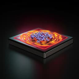
Discover the groundbreaking research on single-layer nanoscale holographic perceptrons conducted by Elena Goi, Xi Chen, Qiming Zhang, Benjamin P. Cumming, Steffen Schoenhardt, Haitao Luan, and Min Gu. These innovative devices, capable of exceeding 500 million neurons per square centimeter, hold remarkable potential in optical data processing and applications in decryption and medical diagnostics.
Related Publications
Explore these studies to deepen your understanding
Adjacent work that informs or extends this paper's methodology and findings.

Engineering and Technology
A touchless user interface based on a near-infrared-sensitive transparent optical imager
T. Kamijo, A. J. J. M. V. Breemen, et al.
Engineering and Technology
A mid-infrared lab-on-a-chip for dynamic reaction monitoring
B. Hinkov, F. Pilat, et al.

Medicine and Health
Toward optical coherence tomography on a chip: in vivo three-dimensional human retinal imaging using photonic integrated circuit-based arrayed waveguide gratings
E. A. Rank, R. Sentosa, et al.
Engineering and Technology
Design and fabrication of a vigorous “cavitation-on-a-chip” device with a multiple microchannel configuration
F. R. Talabazar, M. Jafarpour, et al.


