Engineering and Technology
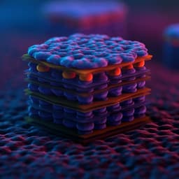
Layer-dependent Schottky contact at van der Waals interfaces: V-doped WSe₂ on graphene
S. Stolz, A. Kozhakhmetov, et al.
This exciting research by Samuel Stolz and colleagues delves into the enhancements provided by van der Waals semimetals when interfaced with 2D semiconductors, revealing how heavily doped WSe₂ exhibits unique charge dynamics as thickness varies, influencing contact resistance significantly.
Related Publications
Explore these studies to deepen your understanding of the subject.