Engineering and TechnologyNature Communications
Large-area transfer of two-dimensional materials free of cracks, contamination and wrinkles via controllable conformal contact
Y. Zhao, Y. Song, et al.
Discover a revolutionary technique that enables the transfer of two-dimensional materials onto any surface without the hassles of cracks, contamination, or wrinkles. Achieving ultraclean surfaces and incredibly high carrier mobilities, this cutting-edge research was conducted by a team of experts including Yixuan Zhao, Yuqing Song, Zhaoning Hu, and many more.
Related Publications
Explore these studies to deepen your understanding
Adjacent work that informs or extends this paper's methodology and findings.
Medicine and Health
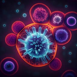
Rapid and stain-free quantification of viral plaque via lens-free holography and deep learning
T. Liu, Y. Li, et al.

Engineering and Technology
Direct electrosynthesis and separation of ammonia and chlorine from waste streams via a stacked membrane-free electrolyzer
J. Gao, Q. Ma, et al.
Physics
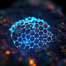
Understanding the impact of heavy ions and tailoring the optical properties of large-area monolayer WS<sub>2</sub> using focused ion beam
F. Sarcan, N. J. Fairbairn, et al.
Engineering and Technology
Transfer-free rapid growth of 2-inch wafer-scale patterned graphene as transparent conductive electrodes and heat spreaders for GaN LEDs
F. Xiong, J. Sun, et al.


