logo
ResearchBunny Logo
Bright and dark Talbot pulse trains on a chip

Engineering and Technology

Bright and dark Talbot pulse trains on a chip

J. Wu, M. Clementi, et al.

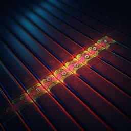
Discover the groundbreaking work by Jiaye Wu and colleagues at EPFL, demonstrating a silicon nitride integrated photonic device that produces two-fold self-images of pulse trains using the temporal Talbot effect. This innovative device doubles the repetition rate of optical combs, paving the way for advanced system-on-chip integration of pulse multipliers.

00:00
00:00
~3 min • Beginner • English
Introduction
The Talbot effect, first reported by H. F. Talbot in 1836 as a spatial self-imaging phenomenon, has since been generalized to temporal, spectral, and azimuthal domains, unified by space-time dualities. Temporal Talbot effects enable applications such as integer/fractional/arbitrary repetition-rate multiplication (RRM), broadband invisibility, and noiseless intensity amplification, and are especially attractive in extra-cavity contexts (communications, passive amplification, microwave photonics) via spectral amplitude and/or phase filtering. Prior work has focused largely on bright pulse trains; dark-pulse Talbot patterns at higher RRMs have only recently been explored. A hybrid Mach-Zehnder interferometer (MZI) and delay-line interferometer (DLI) approach has been proposed for scalable on-chip Talbot processing. Photonic integration is critical for future systems, with integration advances in sources, amplifiers, and signal-processing. While Talbot effects have been used on-chip in microscopy, spectroscopy, and Talbot-cavity lasers, on-chip temporal Talbot generation remains scarcely reported. A recent silicon Bragg-grating phase filter demonstrated spectral phase control, but with limited tunability and challenges for lower repetition rates due to quadratic dispersion-length scaling. Moreover, dark-pulse Talbot processing has not been demonstrated in integrated optics. This work addresses these gaps by designing and experimentally demonstrating a silicon nitride Talbot photonic integrated circuit (PIC) based on cascaded MZI-DLI to imprint Talbot phase onto in-phase combs and realize 2× self-images for both bright and dark pulse trains while preserving amplitude spectra. The approach scales linearly in delay length with inverse repetition rate, enabling lower-rate operation, and includes thermo-optic tuning to switch between pass-through and RRM outputs.
Literature Review
Extensive studies have established Talbot self-imaging across temporal, spectral, and azimuthal domains, unified by duality principles (space-time, time-frequency). Temporal Talbot effects have enabled RRM, invisibility, and coherent amplification, commonly realized via spectral amplitude and/or phase filtering, often with bulk components or programmable pulse shapers. Dark-pulse Talbot behavior was only recently observed and analyzed in fiber/bulk systems. On-chip Talbot-related implementations prior to this work include microscopy, spectroscopy, and Talbot-cavity lasers for coherent coupling, but not temporal Talbot processing of combs. A notable on-chip approach used silicon waveguide Bragg gratings as dispersive phase filters, yet suffered from limited tunability and scalability to lower repetition rates, since dispersion-based Talbot processors require device length scaling quadratically with inverse repetition rate. Tapped delay-line architectures combining amplitude and phase filtering have been proposed for Talbot processing and can, in principle, be integrated via MZI/DLI networks for scalable Nx RRM.
Methodology
Theory: The temporal Talbot phase relation for a comb with mode index k is φ_k = π(p/q)k^2, with p and q coprime. Using quadratic Gauss sums, the phase of each self-image satisfies φ_n = −π(s n^2 + c), with s and c determined by p and q depending on q parity. For 2× RRM (p/q = 1/2), the target line-by-line phase across comb lines is [..., π/2, 0, π/2, 0, ...], preserving the amplitude spectrum. Implementing Talbot phases via an N-parallel tapped delay-line interferometric structure combines spectral amplitude filtering (for Nx RRM) and phase-only filtering (to preserve the spectrum). For N = 2, using the generalized Landsberg–Schaar identity, the combined transfer function yields an imparted phase pattern matching the required Talbot phase for 2× RRM. The effective delay τ_delay sets the imparted phase and the DLI free-spectral range (FSR), with required length scaling linearly with 1/Δν, unlike dispersion-based approaches scaling as 1/Δν^2. Chip design and fabrication: A Si3N4 PIC (fabricated via LIGENTEC MPW) integrates a two-stage cascaded MZI: (i) a thermo-optically tunable first-stage MZI for power balancing and pass-through control; (ii) a second-stage unbalanced MZI acting as a DLI with 125 ps arm delay (half-period of a 4 GHz input) and a thermo-optic phase shifter for recombination phase control. Waveguides are 1.6 × 0.8 μm Si3N4 embedded in SiO2 on Si; fundamental TE mode n_eff ≈ 1.6769 at 1550 nm. Parallel waveguide separation is 22 μm. 2×2 MMI couplers provide nominal 50:50 splitting. Heaters are 50 Ω resistive thermo-optic actuators. The interferometric transmission exhibits an FSR designed at 8 GHz, tunable via heaters (visibility from 0 to 1 via first phase shifter; spectral alignment via DLI heater). Experimental setup: A tunable C-band CW laser (~10 dBm) is intensity-modulated by a LiNbO3 1×2 MZM driven by a quasi-Nyquist RF synthesis of 4 GHz from 4/8/12 GHz harmonics (RF sources and amplifier specified). The MZM produces complementary bright and dark 4 GHz pulse trains (FWHM ~50 ps); one output is used at a time. The chip is temperature-stabilized at 25 °C using a Peltier-controlled stage. On-chip heaters control the first-stage splitting (pass-through vs Talbot operation) and the DLI recombination phase. Outputs are characterized by an optical spectrum analyzer (OSA) and a high-bandwidth oscilloscope (OSC) with 20 GHz optical module. Phase retrieval: The device phase transmission in Talbot mode is reconstructed from the measured amplitude transmission (FSR trace) via a Hilbert transform (causality-based analytic relation akin to Kramers–Kronig), enabling extraction of the comb-line phases for comparison with the theoretical [..., π/2, 0, ...] pattern. Instruments: Specific RF sources (Anritsu MG3692C, Agilent E8257D, Agilent MXG N5183A), amplifier (Mini-Circuits ZVA-0.5W303G+), MZM (EOSPACE AX-1×2-OMSS-20), EDFA (Optilab EDFA-16-LC-M), tunable laser (Yenista Tunics-T100S-HP), OSA (APEX AP2043B), oscilloscope (Agilent Infiniium DCA 86100A with 86105A). Data and code availability: DOI links provided for datasets and code.
Key Findings
- First proof-of-principle on-chip temporal Talbot processor in Si3N4 demonstrating 2× repetition-rate multiplication (RRM) for both bright and dark pulse trains while preserving the comb amplitude spectrum. - Repetition rate doubling: 4 GHz input pulse trains converted to 8 GHz output. The DLI delay is 125 ps (1/2 × 1/4 GHz). - Temporal profiles: Bright pulses maintain FWHM ~50 ps at 8 GHz; dark-pulse 8 GHz trains exhibit slightly reduced FWHM and uneven DC pedestal due to destructive intra-pulse interference between recombined trains. - Spectral preservation: Comb line spacing remains 0.032 nm (~4 GHz at C-band) for both pass-through and Talbot modes, with no loss of frequency components or bandwidth change between modes; minor discrepancies attributed to laser jitter and amplifier noise. - Interferometric control: Thermo-optic tuning in the first-stage MZI switches between pass-through and Talbot modes. Operational power sweep shows Talbot operation near 0 mW and again near ~150 mW dissipated power (first-stage heater); pass-through regions between ~40–120 mW; upper safe limit ~180 mW. - Transmission/FSR: Device interferogram FSR designed and measured at 8 GHz, matching the 2× RRM target. - Phase verification: Hilbert-transform-derived phase shows comb-line phases following approximately [..., π/2, 0, π/2, 0, ...], matching Talbot theory. - Scaling advantage: Required delay length scales as L ∝ Δν⁻¹ (MZI-DLI) vs L ∝ Δν⁻² (dispersion-based Talbot), favoring lower repetition-rate operation. - Broadband considerations: MMI couplers provide ~40 nm 3 dB bandwidth; within band, splitting is near ideal; outside bandwidth, imbalance arises. - Efficiency: In a single-output collection, output power is ~1/N (N = 2 here → 3 dB). If both outputs are collected (2×2 DFT star network behavior), total efficiency approaches 100% (excluding coupling losses) and outputs are mutual coherent copies (up to a constant phase). - Compatibility with other inputs: The same 125 ps delay supports odd multiples of 4 GHz inputs (e.g., 12, 20, 28 GHz), theoretically yielding 2× outputs with Talbot phase preserved. - Comparative metrics: For dispersion-based SMF Talbot at 4 GHz, p/q = 1/2 would require ~230.26 km of SMF (β2 ≈ −21.6 ps²/km), highlighting the compactness of the 4.94 mm PIC. State-of-the-art Bragg-based Talbot chips (2× at 10 GHz) are longer (~8 mm; linearly chirped ~4 cm) and would need to be >4× larger to operate at 4 GHz.
Discussion
This work demonstrates that the temporal Talbot effect can be realized on an integrated Si3N4 PIC using a cascaded MZI-DLI architecture to impart the required quadratic phase across comb lines, thereby doubling repetition rate while conserving the amplitude spectrum. The experimental observations—unchanged comb spacing, preserved spectral bandwidth, temporal 4→8 GHz transformation for both bright and dark pulses, and comb-line phase measurements matching [..., π/2, 0, ...]—directly validate the Talbot condition and address the challenge of achieving RRM without spectral distortion on-chip. The thermo-optic control provides reconfigurability between pass-through and Talbot modes, and the architecture’s linear scaling of required delay with inverse repetition rate improves accessibility for low-rate combs where dispersion-based approaches become impractically long. Efficiency considerations are addressed by recognizing the dual-output nature of the interferometric recombiner; both outputs can be used or coherently recombined to recover near-lossless operation, a hallmark of Talbot processing. The device shows potential for broadband operation within the MMI bandwidth and forms a compact, integrable building block for system-on-chip photonics, with implications for communications, passive amplification, microwave photonics, and optical clock distribution. Theoretical compatibility with other (odd-multiple) input repetition rates and prospects for cascading/parallelization suggest scalability to higher RRM factors, provided appropriate control and calibration are implemented.
Conclusion
A silicon nitride PIC based on cascaded MZI and DLI has been proposed and experimentally validated to implement the temporal Talbot effect on-chip, providing 2× repetition-rate multiplication for both bright and dark optical pulse trains while preserving their spectra. The chip is electrically reconfigurable between pass-through and Talbot modes, demonstrates phase conformity to Talbot theory, and offers favorable scaling (L ∝ Δν⁻¹) for lower repetition-rate inputs in a compact 4.94 mm form factor. This is the first on-chip demonstration of the temporal Talbot effect for dark pulses. The approach is compatible with multiple input repetition rates (odd multiples of 4 GHz) and, in principle, scalable to higher RRM by increasing the number of delay lines. Future directions include multi-stage/parallel MZI-DLI architectures for higher N, integrated packaging to minimize coupling losses and improve spectral fidelity, dispersion management for ultrashort broadband pulses, and closed-loop self-tuning (e.g., machine learning) to mitigate fabrication non-uniformities and automate heater control for robust large-scale Talbot processors.
Limitations
- Bandwidth: 2×2 MMI couplers exhibit ~40 nm 3 dB bandwidth; outside this range, splitting imbalances degrade performance. - Dispersion for ultrashort pulses: The DLI’s finite dispersion may distort very broadband pulses, requiring additional dispersion compensation. - Efficiency in single-output use: Collecting only one output incurs 1/N power scaling (−3 dB for N = 2; more severe for higher N). - Thermal control and fabrication tolerances: Higher-order RRM requires multiple interferometer stages with individual thermal tuning; fabrication non-uniformity can necessitate per-stage calibration and increase control complexity. - Experimental constraints: Demonstrations centered on 4 GHz inputs (hardware-limited); operation at other rates discussed theoretically but not experimentally validated here. - Coupling and propagation losses: Current measurements include chip coupling losses; while SiN propagation loss is low (<0.2 dB/cm), very long delays for very low frequencies can still accumulate loss without careful design. - Operational window: Talbot operation observed within specific heater power regions; stability depends on precise thermal control and may drift without feedback.
Listen, Learn & Level Up
Over 10,000 hours of research content in 25+ fields, available in 12+ languages.
No more digging through PDFs, just hit play and absorb the world's latest research in your language, on your time.
listen to research audio papers with researchbunny