Engineering and TechnologyLight: Science & Applications
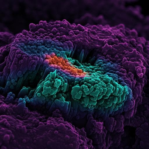
Bottom-up construction of low-dimensional perovskite thick films for high-performance X-ray detection and imaging
S. Dong, Z. Fan, et al.
Discover a groundbreaking method developed by Siyin Dong and colleagues to fabricate high-quality, thick quasi-two-dimensional perovskite films for X-ray detection. Their innovative approach led to significant sensitivity improvements and lower detection limits, revolutionizing advanced imaging technology.
Related Publications
Explore these studies to deepen your understanding
Adjacent work that informs or extends this paper's methodology and findings.
Medicine and Health
Design and Analysis of a Deep Learning Ensemble Framework Model for the Detection of COVID-19 and Pneumonia Using Large-Scale CT Scan and X-ray Image Datasets
X. Xue, S. Chinnaperumal, et al.
Engineering and Technology
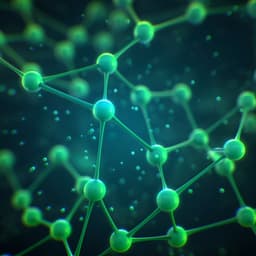
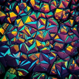
Controlled on-chip fabrication of large-scale perovskite single crystal arrays for high-performance laser and photodetector integration
Z. Xu, X. Han, et al.

Engineering and Technology
Enhanced detection of threat materials by dark-field x-ray imaging combined with deep neural networks
T. Partridge, A. Astolfo, et al.
Biology
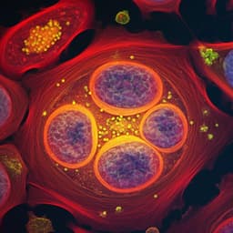
High-dimensional super-resolution imaging reveals heterogeneity and dynamics of subcellular lipid membranes
K. Zhanghao, W. Liu, et al.


