logo
ResearchBunny Logo
All-2D CVD-grown semiconductor field-effect transistors with van der Waals graphene contacts

Engineering and Technology

All-2D CVD-grown semiconductor field-effect transistors with van der Waals graphene contacts

M. A. Hoque, A. George, et al.

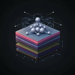
This groundbreaking research by Md. Anamul Hoque and colleagues explores the electronic transport capabilities of a novel all-2D CVD-grown MoS2 field-effect transistor integrated with graphene contacts. Their findings reveal how graphene's tunable Fermi level enhances performance by reducing the Schottky barrier, setting the stage for the future of electronic devices.

00:00
00:00
~3 min • Beginner • English
Abstract
Two-dimensional (2D) semiconductors and van der Waals (vdW) heterostructures with graphene have generated enormous interest for future electronic, optoelectronic, and energy-harvesting applications. The electronic transport properties and correlations of such hybrid devices strongly depend on the quality of the materials via chemical vapor deposition (CVD) process, their interfaces and contact properties. However, detailed electronic transport and correlation properties of the 2D semiconductor field-effect transistor (FET) with vdW graphene contacts for understanding mobility limiting factors and metal-insulator transition properties are not explored. Here, we investigate electronic transport in scalable all-2D CVD-grown molybdenum disulfide (MoS2) FET with graphene contacts. The Fermi level of graphene can be readily tuned by a gate voltage to enable a nearly perfect band alignment and, hence, a reduced and tunable Schottky barrier at the contact with good field-effect channel mobility. Detailed temperature-dependent transport measurements show dominant phonon/impurity scattering as a mobility limiting mechanisms and a gate-and bias-induced metal-insulator transition in different temperature ranges, which is explained in light of the variable-range hopping transport. These studies in such scalable all-2D semiconductor heterostructure FETs will be useful for future electronic and optoelectronic devices for a broad range of applications.
Publisher
npj 2D Materials and Applications
Published On
Aug 21, 2024
Authors
Md. Anamul Hoque, Antony George, Vasudev Ramachandra, Emad Najafidehaghani, Ziyang Gan, Richa Mitra, Bing Zhao, Satyaprakash Sahoo, Maria Abrahamsson, Qiuhua Liang, Julia Wiktor, Andrey Turchanin, Sergey Kubatkin, Samuel Lara-Avila, Saroj P. Dash
Tags
2D semiconductors
van der Waals heterostructures
MoS2
graphene contacts
electronic transport
Schottky barrier
mobility
Listen, Learn & Level Up
Over 10,000 hours of research content in 25+ fields, available in 12+ languages.
No more digging through PDFs, just hit play and absorb the world's latest research in your language, on your time.
listen to research audio papers with researchbunny