
ChemistryLight: Science & Applications
A high mobility air-stable n-type organic small molecule semiconductor with high UV-visible-to-NIR photoresponse
Y. Guan, J. Qiao, et al.
Explore the groundbreaking research conducted by Ying-Shi Guan and colleagues, showcasing high-performance n-type semiconducting crystalline nanosheets. This innovative work reveals air-stable field-effect transistors and phototransistors with unmatched responsivity and detectivity across a broad spectrum, advancing the potential for organic photodetectors.
Related Publications
Explore these studies to deepen your understanding
Adjacent work that informs or extends this paper's methodology and findings.

Physics
High-throughput screening of 2D materials identifies *p*-type monolayer WS₂ as potential ultra-high mobility semiconductor
V. Ha and F. Giustino
Medicine and Health
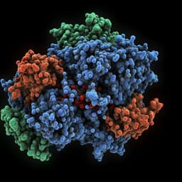
A small molecule compound with an indole moiety inhibits the main protease of SARS-CoV-2 and blocks virus replication
S. Hattori, N. Higashi-kuwata, et al.

Engineering and Technology
Ubiquitous organic molecule-based free-standing nanowires with ultra-high aspect ratios
K. Kamiya, K. Kayama, et al.

Chemistry
Free charge photogeneration in a single component high photovoltaic efficiency organic semiconductor
M. B. Price, P. A. Hume, et al.


