Engineering and TechnologyNature Communications
Transparent near-infrared perovskite light-emitting diodes
C. Xie, X. Zhao, et al.
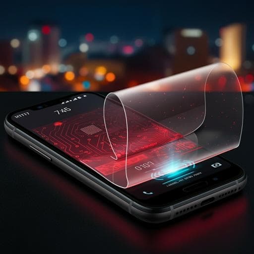
This groundbreaking research reports on the development of a transparent perovskite light-emitting diode (LED) that emits near-infrared light, perfect for enhancing mobile and wearable devices without sacrificing display space. Conducted by Chenchao Xie, Xiaofei Zhao, Evon Woan Yuann Ong, and Zhi-Kuang Tan from the National University of Singapore, this innovation showcases over 55% average transmittance in the visible spectrum.
Related Publications
Explore these studies to deepen your understanding
Adjacent work that informs or extends this paper's methodology and findings.

Chemistry
Towards efficient near-infrared fluorescent organic light-emitting diodes
A. Minotto, I. Bulut, et al.

Engineering and Technology
High efficiency pure blue perovskite quantum dot light-emitting diodes based on formamidinium manipulating carrier dynamics and electron state filling
L. Gao, Y. Zhang, et al.

Engineering and Technology
Efficient and stable hybrid perovskite-organic light-emitting diodes with external quantum efficiency exceeding 40 per cent
L. Kong, Y. Luo, et al.

Engineering and Technology
A touchless user interface based on a near-infrared-sensitive transparent optical imager
T. Kamijo, A. J. J. M. V. Breemen, et al.


