Engineering and TechnologyMicrosystems & Nanoengineering
Nondestructive monitoring of annealing and chemical-mechanical planarization behavior using ellipsometry and deep learning
Q. Sun, D. Yang, et al.
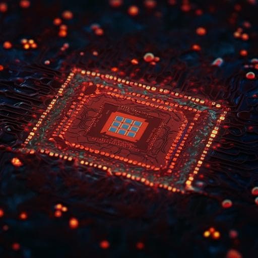
Discover a groundbreaking nondestructive defect inspection method for through-silicon via structures that leverages Mueller matrix spectroscopic ellipsometry and deep learning. This innovative technique, crafted by Qimeng Sun, Dekun Yang, Tianjian Liu, Jianhong Liu, Shizhao Wang, Sizhou Hu, Sheng Liu, and Yi Song, demonstrates astonishing accuracy rates in identifying defects, promising rapid evaluations for advanced manufacturing processes.
Related Publications
Explore these studies to deepen your understanding
Adjacent work that informs or extends this paper's methodology and findings.
Medicine and Health
Design and Analysis of a Deep Learning Ensemble Framework Model for the Detection of COVID-19 and Pneumonia Using Large-Scale CT Scan and X-ray Image Datasets
X. Xue, S. Chinnaperumal, et al.

Medicine and Health
Recent Advancements and Perspectives in the Diagnosis of Skin Diseases Using Machine Learning and Deep Learning: A Review
J. Zhang, F. Zhong, et al.

Biology
Experimental exploration of a ribozyme neutral network using evolutionary algorithm and deep learning
R. Rotrattanadumrong and Y. Yokobayashi

Chemistry
Design of target specific peptide inhibitors using generative deep learning and molecular dynamics simulations
S. Chen, T. Lin, et al.


