
Engineering and TechnologyNature Communications
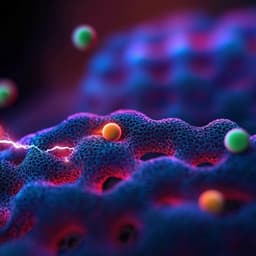
Nanotransistor-based gas sensing with record-high sensitivity enabled by electron trapping effect in nanoparticles
Q. Hu, P. Solomon, et al.
Discover the groundbreaking research by Qitao Hu, Paul Solomon, Lars Österlund, and Zhen Zhang on ultra-sensitive, low-power H₂ gas sensors using nanoscale FETs with Pd nanoparticles. Their innovative approach achieves record-high responses and low detection limits, revolutionizing gas sensing technology.
Related Publications
Explore these studies to deepen your understanding
Adjacent work that informs or extends this paper's methodology and findings.

Engineering and Technology
High-sensitivity nanophotonic sensors with passive trapping of analyte molecules in hot spots
X. Miao, L. Yan, et al.
Engineering and Technology
Biodegradable, flexible silicon nanomembrane-based NOx gas sensor system with record-high performance for transient environmental monitors and medical implants
G. Ko, S. D. Han, et al.

Medicine and Health
The effect of mindfulness-based cognitive therapy on rumination and a task-based measure of intrusive thoughts in patients with bipolar disorder
J. Lubbers, D. Geurts, et al.

Environmental Studies and Forestry
High-ambition climate action in all sectors can achieve a 65% greenhouse gas emissions reduction in the United States by 2035
A. Zhao, K. T. V. O’keefe, et al.


