Physics
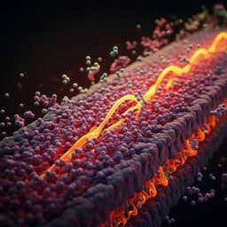
Highly efficient photoelectric effect in halide perovskites for regenerative electron sources
F. Liu, S. Sidhik, et al.
Discover groundbreaking advancements in electron sources with innovative halide perovskite thin films, demonstrating remarkable quantum efficiency and longevity. This research, conducted by a team including Fangze Liu, Siraj Sidhik, and others, paves the way for versatile and cost-effective applications in various fields.
~3 min • Beginner • English
Introduction
The study addresses whether solution-processed halide perovskite thin films can serve as efficient, durable, low-cost photoelectron sources (photocathodes) when excited at or above their bandgap. Halide perovskites have rapidly advanced in optoelectronics due to low-cost processing, tunable properties, and excellent charge transport, rivaling traditional inorganic semiconductors in several applications. Conventional photocathodes (metals, alkali antimonides/tellurides, III-V semiconductors) present trade-offs between high quantum efficiency (QE) and operational lifetime, and typically require ultra-high vacuum (UHV) and complex surface conditioning (e.g., NEA via Cs and oxidant for GaAs). The stringent requirements and costs motivate exploration of new semiconductors that could simplify fabrication/operation and tolerate higher vacuum pressures. The authors propose and investigate halide perovskite thin films as photoelectron emitters, examining efficiency, spectral tunability, operational stability, and the ability to regenerate emission through simple Cs surface activation.
Literature Review
State-of-the-art photocathodes include metals (e.g., Cu, Mg, Pb) with long lifetimes but low QE (~0.1% or less), and non-metal semiconductors (alkali antimonides/tellurides like Cs2Te, K2CsSb, Cs3Sb; III-Vs like GaAs, GaN) achieving QE >10% after careful surface preparation to enable negative electron affinity (NEA), often via Cs deposition and an oxidant. These high-QE devices typically require UHV (10^-11–10^-12 torr) and atomically clean, high-quality crystalline surfaces; residual gases (H2O, O2, CO2) degrade performance. GaAs, for example, achieves high QE under NEA but is highly sensitive to contamination, with reported low gas exposure tolerances. GaN can be somewhat more tolerant in certain cases. Recent studies report perovskite thin films have work functions around ~4.0–4.1 eV with Fermi level pinning relatively insensitive to composition, and bulk ionization energy in CsPbBr3 near ~5.8 eV. Prior perovskite literature establishes strong charge transport, long diffusion lengths, and potential for device-grade optoelectronics, motivating their assessment as photocathodes.
Methodology
Materials and film fabrication: CsPbX3 (X = Br or I) thin films were prepared by solution processing under Ar glovebox conditions. For CsPbBr3, equimolar PbBr2 and CsBr in DMSO (0.4 M) were spin-coated at 2000 rpm; for CsPbI3, equimolar PbI2 and CsI in DMF (0.6 M) were spin-coated at 3000 rpm, targeting ~200 nm thickness. Films were annealed at 100 °C for 10 min. Hybrid perovskites included FA0.7MA0.25Cs0.05PbI3 (0.43 M in DMSO) and 2D Ruddlesden-Popper BA2MAn−1PbnI3n+1 (n=2,5) prepared by hot-casting; layered crystals were synthesized via literature methods by dissolving PbO in HI/H3PO2, then adding MAI and BA, and crystallizing upon cooling. Doped Si substrates (1 in^2, 0.001–0.005 Ω·cm, ~500 µm) were O2 plasma treated before coating. Samples were transferred to vacuum with <5 min air exposure. In UHV load lock, only CsPbBr3 and CsPbI3 were baked at 350 °C for 24 h to remove residues; hybrids were not baked to avoid organic sublimation and degradation. Main chamber base pressure was ~1×10^-9 torr with residual partial pressures ~1.6×10^-11 (H2O), 3.8×10^-11 (O2), 3.5×10^-11 torr (CO2).
Photoelectric effect measurements: A Newport 150 W Xe lamp with monochromator (300 l/mm grating) and long-pass filters provided monochromatic illumination from 1.55 to 4.96 eV (800–250 nm), modulated at 400 Hz. The beam entered at 45° through a quartz window, illuminating ~10 mm^2 with 38–50 µW power (QE independent of intensity in this regime). An anode 25 mm from the film was biased at +90 V relative to the doped Si substrate; the chamber was tied to anode potential to suppress chamber emission. A 100 kΩ series resistor converted photocurrent to voltage; total capacitance 2.7 nF (τ=0.27 ms). Signal was read by an SR830 lock-in with 0.3–10 s time constant. Spatial QE maps used a 405 nm laser scanned by a steering mirror.
Cesium activation: Cs was deposited in situ using a 1 cm SAES dispenser. The source was degassed at 4 A, then positioned 2.5–5 cm from the sample. While monitoring 405 nm photocurrent, current was ramped at 0.1 A/min; QE typically increased starting at 4.5–5 A. Current was held/adjusted to maximize QE, stopping before overcoating (which reduced QE). The dispenser was retracted and turned off, followed immediately by spectral QE scans. Evidence suggests a few monolayers of Cs with inhomogeneous thickness form, with thick Cs layers degrading QE and no emission from Cs itself.
Surface analysis: Auger electron spectroscopy (AES) employed a SPECS Phoibos 150 analyzer with MCD-5 detector. Electron gun: 3 keV, 1 µA, ~1 mm^2 spot. AES chamber connected to Cs deposition chamber via transfer arm. AES before/after UHV annealing showed unchanged Cs, Br, Pb peaks and significantly reduced C and O peaks, confirming effective surface cleaning without altering perovskite chemistry. Cs coverage was quantified via Cs(49 eV)/Br(55 eV) Auger peak ratio. Internal quantum efficiency (IQE) was evaluated as QE divided by absorbance.
Key Findings
- Demonstration of efficient photoelectron emission from solution-processed halide perovskite thin films (CsPbBr3, CsPbI3, and hybrid perovskites), with spectral tunability across visible–UV.
- Cs activation induces a 3–4 orders of magnitude QE increase and reduces the emission onset from ~4.0 eV (pristine) to near the bandgap: ~2.1 eV for CsPbBr3 and ~1.8 eV for CsPbI3, indicating negative electron affinity at the surface.
- Peak QE: 2.2% at 5.0 eV for CsPbBr3; 0.14% at 3.5 eV for CsPbI3. For CsPbBr3, QE >1% for photon energy >3.9 eV and >0.25% at 3.1 eV (400 nm).
- Reproducibility: 17 CsPbBr3 films showed average maximum QE >1.5%, with two champions >2% at 5 eV.
- Hybrid perovskites (FA0.7MA0.25Cs0.05PbI3; BA2MA1Pb2I7; BA2MA4Pb5I16) exhibited emission after Cs activation with onsets near their bandgaps (e.g., BA2MAn−1PbnI3n+1 onset ~2.35 eV vs optical Eg ~2.18 eV) and QE ~0.01% between 3–3.5 eV, outperforming metals by ~2 orders in this range.
- Mechanism: IQE mirrors QE, indicating photogeneration/absorption not limiting. Transport is efficient in 3D perovskites (μτ ~10^-2–10^-4 cm^2/V; long diffusion lengths). Limiting step is electron escape at the surface (step iii), governed by surface recombination velocity and surface barriers. Cs deposition forms a surface dipole, lowers work function, and drives negative electron affinity, enabling efficient emission.
- AES and theory: Cs coverage increased QE continuously up to ~2.5 Cs/unit cell (max QE), consistent with DFT showing lower work function for two Cs layers than one; further Cs reduces QE. Pristine work functions ~4.0 eV across compositions, consistent with Fermi-level pinning by surface states.
- Stability: Under continuous illumination at 3.06 eV and base pressure ~1×10^-9 torr, QE decreased to ~60% after 25 h and ~8% after 96 h. Estimated 63% decay exposures: 2.86 L (H2O), 6.75 L (O2), 6.28 L (CO2), indicating higher gas tolerance than many semiconductor photocathodes at similar pressures.
- Regeneration: Post-degradation, in situ Cs deposition restored QE to near-original values within ~1 h. AES showed Cs coverage decreased from 2.5 to 2.1 Cs/unit cell upon degradation with ~30% rise in O Auger signal; reactivation increased Cs to 2.7 Cs/unit cell and reduced O peak to initial levels. Subsequent activations were ~4× faster than initial, suggesting partial surface compromise mainly at the Cs layer.
- Operational environment: Devices operated at ~10^-9 torr, at least two orders higher pressure (i.e., less stringent vacuum) than typical semiconductor photocathodes.
Discussion
The results establish halide perovskite thin films as promising photocathodes with respectable QE achieved via simple solution processing and a straightforward Cs activation step. By correlating external and internal QE, and considering known transport parameters, the emission efficiency is chiefly limited by surface escape processes rather than bulk absorption or transport in 3D perovskites. Cs deposition creates a surface dipole that lowers the electron affinity to negative values, reducing the emission threshold to near the bandgap and boosting QE by orders of magnitude. The observed universal pristine emission onset (~4.0 eV) across different perovskite compositions supports a picture of Fermi level pinning by similar surface states. Spatial inhomogeneity and sample-to-sample performance variation highlight incomplete control of Cs coverage and surface conditioning. Hybrid perovskites, despite not being UHV annealed due to organic volatility, still show measurable emission after Cs activation, indicating robustness of the approach. Stability tests demonstrate operation for tens of hours at relatively high vacuum pressures, with degradation largely attributable to Cs surface reactions with residual oxygenated gases; this degradation is reversible through rapid, in situ Cs reactivation. Collectively, these findings answer the central question by showing that perovskites can function as efficient, regenerative, spectrally tunable electron sources under relaxed vacuum requirements, offering a pathway toward lower-cost, adaptable photocathodes.
Conclusion
This work demonstrates that solution-processed halide perovskite thin films can serve as efficient, regenerative, and spectrally tunable photoelectron sources. Cs activation leads to negative electron affinity, reducing emission thresholds to near the bandgap and enabling QE up to 2.2% (CsPbBr3) with operation at ~10^-9 torr and lifetimes exceeding 25 h. The electron emission can be fully regenerated after degradation via a simple in situ Cs deposition. Performance is reproducible across multiple samples and extendable to hybrid perovskites. Future research should focus on: (i) refining Cs activation to control coverage/uniformity and stabilize NEA surfaces; (ii) improving film quality and surface passivation to reduce recombination and enhance escape probability; (iii) exploring alternative alkali or co-activation chemistries and encapsulation strategies to further increase stability; and (iv) device engineering (e.g., heterostructures, surface treatments) to approach or surpass III-V photocathode performance at significantly lower cost and with less stringent vacuum requirements.
Limitations
- QE remains below the best III-V photocathodes; surface escape remains the primary limitation.
- Cs activation control is limited, leading to spatial inhomogeneity and variation across samples; optimal coverage is narrow (~2 monolayers).
- Hybrid perovskites could not be UHV annealed due to organic volatility, leaving surface adsorbates that likely blue-shift onset and reduce QE.
- Degradation under residual gases persists; although regenerable via Cs, long-term stability beyond ~96 h and under practical operating conditions needs further validation.
- 2D Ruddlesden-Popper perovskites exhibit lower charge transport (μτ ~10^-6–10^-5 cm^2/V), contributing to lower QE compared to 3D films.
Related Publications
Explore these studies to deepen your understanding of the subject.

