
Engineering and Technologynpj 2D Materials and Applications
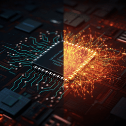
Graphene-based 3D XNOR-VRRAM with ternary precision for neuromorphic computing
B. Alimkhanuly, J. Sohn, et al.
Discover how the innovative use of microfabricated, graphene-based Vertical RRAM (VRRAM) can revolutionize neuromorphic computing, enhancing energy efficiency and recognition accuracy. This exciting research conducted by Batyrbek Alimkhanuly, Joon Sohn, Ik-Joon Chang, and Seunghyun Lee showcases the advantages of graphene in advanced computing technologies.
Related Publications
Explore these studies to deepen your understanding
Adjacent work that informs or extends this paper's methodology and findings.
Computer Science
Spike-based dynamic computing with asynchronous sensing-computing neuromorphic chip
M. Yao, O. Richter, et al.

Engineering and Technology
Electron-beam-irradiated rhenium disulfide memristors with low variability for neuromorphic computing
S. Li, B. Li, et al.

Engineering and Technology
3D printed graphene-based self-powered strain sensors for smart tires in autonomous vehicles
D. Maurya, S. Khaleghian, et al.

Chemistry
Variational autoencoder-based chemical latent space for large molecular structures with 3D complexity
T. Ochiai, T. Inukai, et al.


