Engineering and TechnologyNature Communications
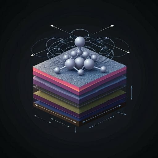
Defect-gradient-induced Rashba effect in van der Waals PtSe₂ layers
J. Jo, J. H. Kim, et al.
This groundbreaking research by Junhyeon Jo, Jung Hwa Kim, Choong H. Kim, and their colleagues unveils the creation of a defect gradient and the Rashba effect in 1T-phase PtSe₂ thin films through plasma treatment. Scanning transmission electron microscopy reveals a unique defect structure, paving the way for advanced electronic applications.
Related Publications
Explore these studies to deepen your understanding
Adjacent work that informs or extends this paper's methodology and findings.
Engineering and Technology
Disorder-induced bulk photovoltaic effect in a centrosymmetric van der Waals material
C. Cheon, Z. Sun, et al.

Physics
Current-induced domain wall motion in a van der Waals ferromagnet Fe3GeTe2
W. Zhang, T. Ma, et al.

Physics
Room temperature energy-efficient spin-orbit torque switching in two-dimensional van der Waals Fe<sub>3</sub>GeTe<sub>2</sub> induced by topological insulators
H. Wang, H. Wu, et al.
Physics
Full phonon dispersion along the stacking direction in nanoscale van der Waals materials by picosecond acoustics
S. Lee, S. Bae, et al.


