Engineering and Technology
Chip-integrated van der Waals PN heterojunction photodetector with low dark current and high responsivity
R. Tian, X. Gan, et al.
The study addresses the need for integrated photodetectors on photonic integrated circuits (PICs) that simultaneously provide low dark current, high responsivity, and fast response. Conventional PIC platforms (silicon, silicon nitride, lithium niobate) cannot monolithically integrate efficient photodetectors because their waveguides must be low-loss, non-absorbing. Hetero-integration of bulk semiconductors (germanium or III–V) via epitaxy or wafer bonding introduces cost and interface challenges and is difficult on dielectric platforms. Prior chip-integrated 2D-material photodetectors are promising due to van der Waals integration without lattice matching, but most use metal–semiconductor–metal geometries leading to high dark current and limited bandwidth; graphene devices suffer from zero bandgap–induced dark current. The research hypothesis is that a van der Waals PN heterojunction formed by stacking naturally p- and n-doped 2D semiconductors on a waveguide can leverage the built-in electric field to suppress dark current, enhance responsivity, and maintain high-speed operation. The work demonstrates a BP/MoTe2 PN heterojunction on a silicon nitride waveguide and evaluates its electrical, optical absorption, and photodetection performance including tunability via electrostatic gating.
- Integration of photodetectors on PICs via heteroepitaxy of germanium or III–V on silicon has yielded decent devices but faces high processing costs and scalability limits; wafer bonding is complex and has interface issues.
- On dielectric PICs (silicon nitride, lithium niobate), epitaxial growth of bulk semiconductors is impractical; only a few bonded detectors have been reported with complicated processes.
- 2D materials enable lattice-mismatch-free integration and broad optoelectronic functionalities. Large-area CVD growth exists, easing fabrication.
- Graphene waveguide photodetectors on silicon/silicon nitride/chalcogenide have achieved >110 GHz bandwidth but suffer high dark current due to zero bandgap.
- A monolayer MoS2 detector on silicon nitride achieved ~10^3 A/W responsivity in the visible, but many 2D detectors on waveguides use metal–semiconductor–metal geometries, leading to high dark current and low bandwidth.
- PN junctions in bulk semiconductors are known to suppress dark current and enhance responsivity/bandwidth but require complex doping processes. Van der Waals PN junctions can be formed by stacking naturally doped 2D materials, potentially offering similar benefits with simpler fabrication and tunability via electrostatic gating.
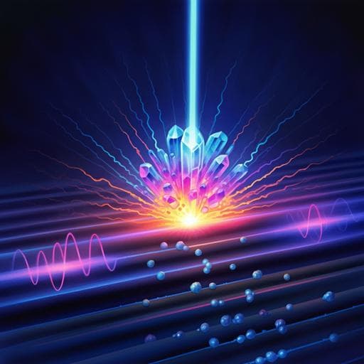
- Device concept: A van der Waals PN heterojunction is formed by stacking p-type black phosphorus (BP) and n-type molybdenum ditelluride (MoTe2). The heterostructure is integrated atop a silicon nitride (Si3N4) waveguide to couple with the evanescent field, extending light–material interaction length for efficient absorption.
- Substrate/waveguide: 300 nm-thick Si3N4 slab on 2 µm SiO2 atop a highly doped Si substrate (used as a global back gate). Waveguide width: 1080 nm for low-loss single-mode operation near telecom wavelengths. Grating couplers are used for in/out coupling.
- Dielectric/encapsulation: h-BN layer under the heterostructure minimizes substrate roughness and potential puddles; a top h-BN layer encapsulates BP/MoTe2 to ensure ambient stability of BP.
- Contacts: Pre-patterned Au pads are peeled from a donor and transfer-printed directly onto BP (drain) and MoTe2 (source); conventional deposition/liftoff would also work. After stacking and contact transfer, the device is annealed in forming gas (95% Ar / 5% H2) to improve interfaces and contact quality.
- Electrostatic gating: With the doped Si back gate and oxide/nitride dielectrics, a vertical field tunes carrier densities, enabling electrostatic doping and junction tunability.
- Material parameters: BP bandgap ~0.3 eV, electron affinity ~4.1 eV; MoTe2 bandgap ~0.9 eV, electron affinity ~3.8 eV, yielding conduction/valence band offsets ~0.3 eV each and a built-in field from MoTe2 to BP at equilibrium. Flake thicknesses: BP ~13 nm, MoTe2 ~10.6 nm. Overlap lengths on the waveguide: BP ~19.77 µm, MoTe2 ~56.6 µm.
- Absorption quantification: A Mach–Zehnder interferometer (MZI) is used with the heterostructure on one arm. Transmission spectra (1500–1630 nm) with TE polarization are recorded after each stacking step to extract extinction ratio changes and deduce absorption. BP absorption coefficient measured ~0.09815 dB/µm (theory ~0.0911 dB/µm), corresponding to ~42.35% absorption over 19.77 µm.
- Electrical/optical measurements: I–V characteristics measured with V_DS from −1 to 1 V in dark and under guided illumination at λ=1503 nm. Photocurrent defined as illuminated minus dark current. Zero-bias short-circuit current (ISC) and open-circuit voltage (VOC) measured to confirm photovoltaic effect. Intrinsic responsivity R_int = I_photo / P_photo_int, where P_photo_int is the BP-absorbed optical power from MZI analysis. Internal quantum efficiency η_QE = R_int × (ħω/q).
- Bandwidth: Frequency response characterized to extract 3 dB bandwidth (reported ~1.0 GHz).
- Strong rectifying diode behavior of the BP/MoTe2 PN junction with ON/OFF current ratio ~1.6 × 10^3 and ideality factor ~1.87 (Shockley fit).
- Low dark current: <7 nA at 1 V bias (polarity from n-type MoTe2 to p-type BP), over two orders of magnitude lower than prior waveguide-integrated BP detectors using M–S–M geometries.
- High responsivity: Intrinsic responsivity up to 577 mA/W; tunable via electrostatic doping to 709 mA/W. At zero bias, R_int ≈ 277 mA/W (self-powered operation).
- Photovoltaic effect: Linear increase of short-circuit photocurrent with absorbed power; open-circuit voltage VOC ≈ 228 mV at BP absorption power 12.79 µW.
- Internal quantum efficiency: ~22.5% at 1503 nm corresponding to the zero-bias responsivity.
- Fast response: Electrical 3 dB bandwidth ~1.0 GHz.
- Broadband on-chip operation across 1500–1630 nm with uniform response.
- Efficient on-chip absorption: BP absorption coefficient ~0.09815 dB/µm; a 19.77 µm BP overlap absorbs ~42.35% of guided power, aiding high responsivity.
- Device architecture and gating demonstrate tunable rectification and improved photodetection performance compared to M–S–M 2D photodetectors and graphene-based devices (which suffer higher dark current).
Forming a van der Waals PN junction between naturally p-doped BP and n-doped MoTe2 creates a built-in electric field that separates photocarriers efficiently, enabling high responsivity and substantial zero-bias photocurrent while suppressing thermally driven dark current compared to M–S–M geometries. The measured rectification (ON/OFF ~1.6×10^3, ideality ~1.87) confirms diode-like behavior responsible for reduced dark current at forward operation. Waveguide integration on Si3N4 extends the light–material interaction length for significant absorption (~42%), supporting high intrinsic responsivity and internal quantum efficiency. Electrostatic back-gating further tunes carrier densities and junction alignment, enhancing rectification and responsivity (to 709 mA/W), demonstrating an additional control knob for performance optimization. The GHz bandwidth indicates that leveraging a PN junction does not preclude fast response, addressing the traditional speed–responsivity trade-off seen in some 2D photodetectors. Broad spectral response (1500–1630 nm) benefits from BP’s narrow direct bandgap, suggesting applicability across telecom bands. Overall, the approach directly addresses the central challenge of achieving low dark current, high responsivity, and fast speed in chip-integrated 2D photodetectors and is compatible with diverse PIC platforms (silicon, silicon nitride, lithium niobate, polymers).
The work demonstrates a silicon-nitride-waveguide-integrated van der Waals PN heterojunction photodetector using p-type BP and n-type MoTe2 that achieves simultaneously low dark current (<7 nA at 1 V), high intrinsic responsivity (up to 577 mA/W; 709 mA/W with electrostatic tuning), self-powered operation with substantial zero-bias responsivity (~277 mA/W) and IQE (~22.5%), ~1.0 GHz bandwidth, and broadband response (1500–1630 nm). The built-in field of the PN junction suppresses dark current and enhances carrier separation, while waveguide coupling and device architecture yield strong on-chip absorption. This strategy offers a scalable path toward high-performance on-chip photodetectors across multiple PIC platforms. Future work could explore: (i) alternative 2D material combinations to target other spectral ranges; (ii) optimization of junction engineering and electrostatic gating for higher speed and responsivity; (iii) scalable fabrication via large-area CVD-grown 2D materials; and (iv) integration in complex PICs for applications in communications, sensing, and computing.
- Environmental stability: BP is air-sensitive, necessitating h-BN encapsulation; long-term reliability in varying environments should be assessed.
- Interface quality: Performance depends on clean, high-quality van der Waals interfaces and low-resistance contacts; transfer processes and bubbles can degrade performance without careful annealing.
- Measurement range: Demonstrations focus on 1500–1630 nm; broader spectral characterization and visible/shortwave IR validation (including MoTe2 contribution) would strengthen generality.
- Scalability: The device uses mechanical exfoliation and transfer-print contacts; transitioning to wafer-scale CVD growth and standard lithographic metallization is required for large-scale production.
- Bandwidth: While ~1.0 GHz is significant, faster operation may be achievable with further device capacitance/resistance optimization; detailed speed limitations (RC vs transit time) are not fully dissected here.
Related Publications
Explore these studies to deepen your understanding of the subject.